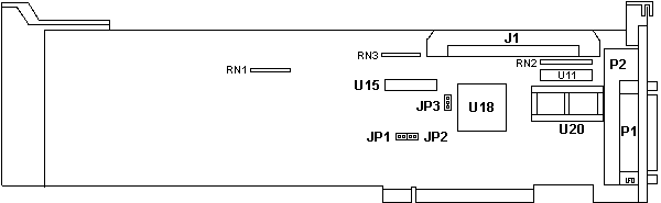
| J1 50 pin header
JP1 Unk Unpopulated JP2 Unk, unpopulated JP3 Bottom two pads shunted. P1 DB25 port P2 solder pads for 50 positions |
RN1-3 Resistor Networks
U11 AMD DP8303N U15 NS DM74LS240N Oops, logic. U18 Chips P82C612 U20 BIOS 0 |
Notes:
No oscillator, clock might be generated by Chips P82C612...
J1 outline hints at a previous configuration of a right angle socket
with retentive catches.
P2 has the solder pads for 50 positions, while P1 is a DB25. Maybe
there was a different external port?