| Parent |
WARNING: |
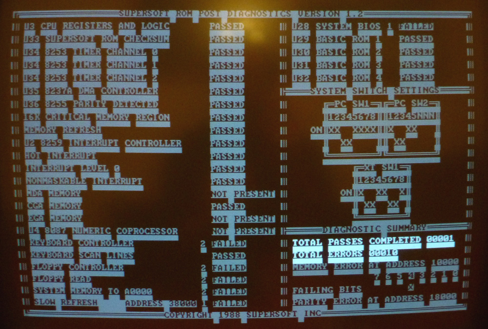
The Supersoft/Landmark Diagnostic ROM is not known to detect RAM addressing problems. ( The POST in the IBM BIOS detects some. ) ( For PC's and XT's, Ruud's Diagnostic ROM detects most. ) |
| Bank 0: | 64 KB sized, | addressed 00000 to 0FFFF hex | ( 0 KB to 64 KB) (soldered to motherboard) |
| Bank 1: | 64 KB sized, | addressed 10000 to 1FFFF hex | ( 64 KB to 128 KB) (socketed) |
| Bank 2: | 64 KB sized, | addressed 20000 to 2FFFF hex | (128 KB to 192 KB) (socketed) |
| Bank 3: | 64 KB sized, | addressed 30000 to 3FFFF hex | (192 KB to 256 KB) (socketed) |
| • | Some video cards will not work with this PC (and XT) version of the Supersoft/Landmark ROM. - My IBM MDA card works. - My IBM CGA card works. - My IBM EGA card will display, but poorly. - My unbranded clone MDA card works. - My unbranded clone CGA card works. - None of my VGA cards work. More information here. |
| • | If a RAM error at address 05040 is reported, note that the "05040" bit is incorrect. Do not believe the "05040" - the diagnostics have displayed the wrong address. |
| • | The SYSTEM MEMORY TO A0000 test will fail if 640 KB (A0000 hex = 640K) of RAM is not fitted. So, that is 256 KB on the motherboard plus 384 KB on an expansion card. RAM related switches on the motherboard are ignored (switches SW1:3 and SW1:4, and SW2). If the only RAM fitted is the 256 KB on the motherboard, expect to see errors when the test advances past address 40000 (256K = 40000 hex). |
| • | The KEYBOARD CONTROLLER test will fail if no PC-class keyboard is connected to the 5150 motherboard. |
| • | The FLOPPY CONTROLLER test requires that a floppy controller card is fitted to the 5150 motherboard. For this test, the card does not need any drives connected to it. |
| • | The FLOPPY READ test takes about 1.5 minutes to fail. Be patient. |
| • | The NONMASKABLE INTERRUPT test will fail if the math coprocessor (8087) is absent and you have switch 2 on SW1 in the wrong position for that (off). |
| • | The U28 ROM test is expected to fail, because there is nothing in the U28 socket. However, on some IBM 5150 motherboards, the test might pass. You may even see it pass sometimes, and fail at other times. |
| • | The MEMORY REFRESH test may not reveal a memory refresh problem - see here. |
| • | It is observed that when a test fails, the Supersoft/Landmark ROM switches the motherboard relay on/off three times. (The clicks are very audible.) |
| • | The settings of the switches within SW1 on the 5150 motherboard are ignored, except for switch 2. |
| • | The settings of the switches within SW2 on the 5150 motherboard are ignored. |
| • | Switches 3 and 4 within SW1 on the IBM 5150 motherboard do not enable/disable RAM banks. The 4 motherboard banks are always enabled. That is why in the IBM 5150, all motherboard RAM banks must be populated before RAM is added via expansion card/s. |
| • | Ignore the box labelled, "XT SW1". That is for when the ROM is used in an IBM 5160 (IBM XT). |
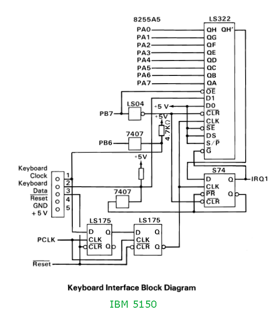
| • | The term 'KEYBOARD CONTROLLER' is misleading. Unlike the IBM 5170, the IBM 5150 does not have a keyboard controller chip. Discrete components are used instead. |
| • | There is nothing in the manual that indicates that codes are sent to port 80h. |
| • | If you are using the Supersoft/Landmark Diagnostic ROM because the IBM 5150 appears 'dead', and you have discovered that the Supersoft/Landmark Diagnostic ROM is running fine, then see note 2 below. |
| Type of EPROM for IBM 5150 | Size | Image download | Photo | Comment |
|---|---|---|---|---|
| MCM68766 EPROM | 8 KB | Download | ||
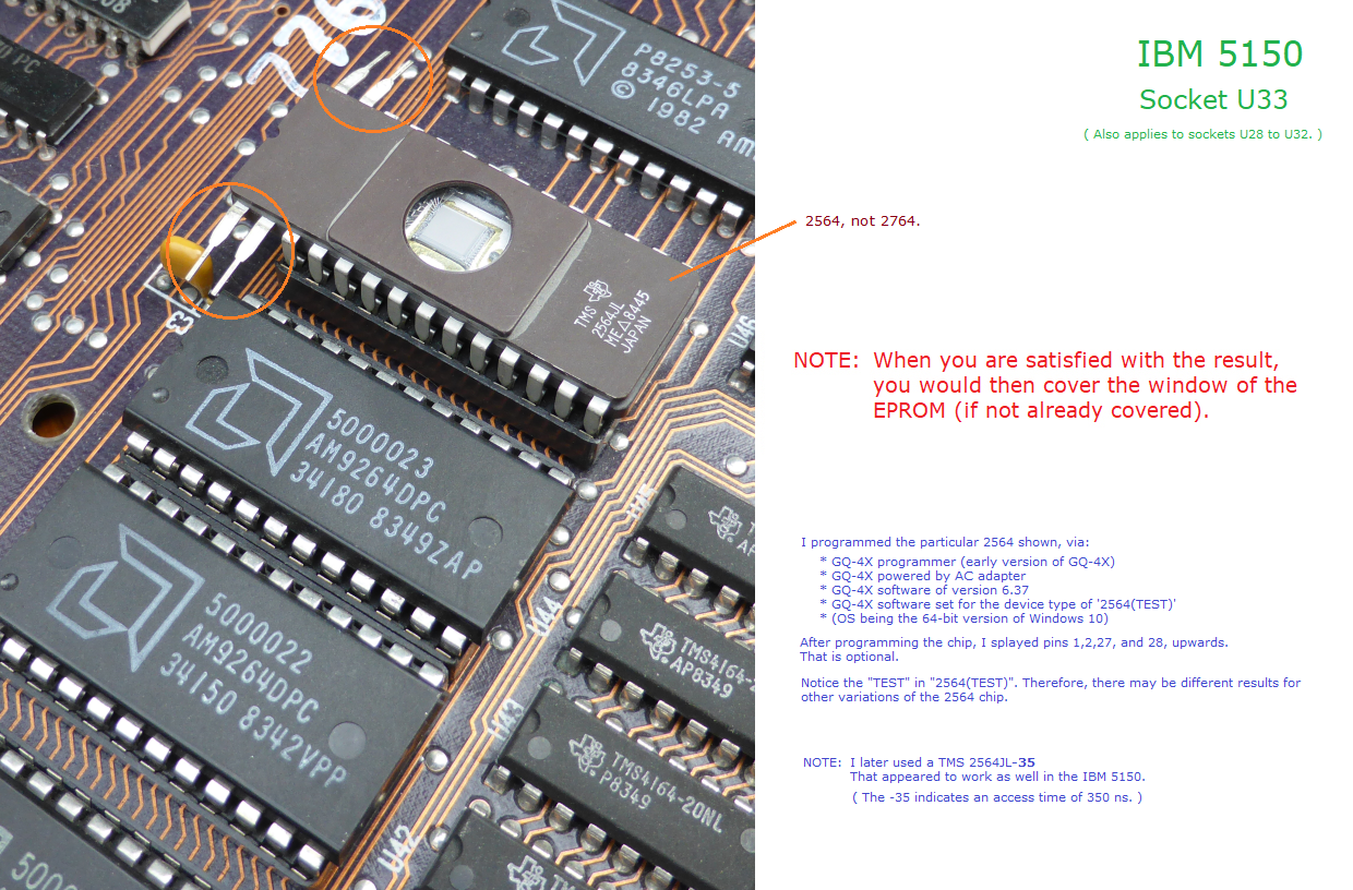
| 2564 EPROM | 8 KB | Download | Photo | 2564, not 2764 |
| With adapter, 2764/27C64 EPROM | 8 KB | Download | Click here for adapter. | |
| With adapter, 27128/27C128 EPROM | 16 KB | Download | Click here for adapter. | |
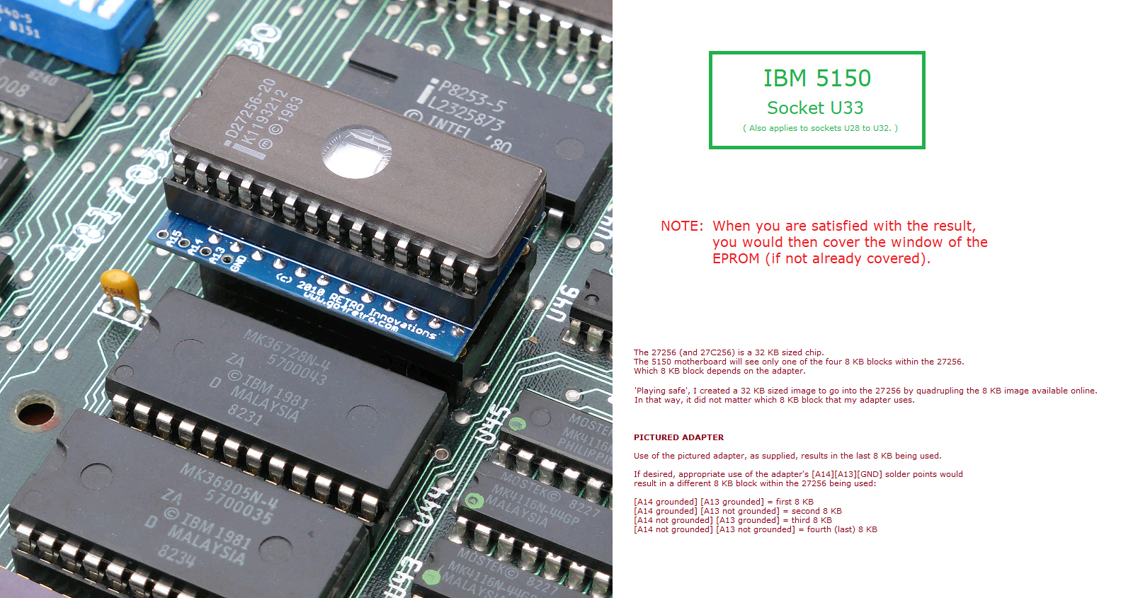
| With adapter, 27256/27C256 EPROM | 32 KB | Download | Photo | Click here for adapter. |
| With adapter, W27E257 EEPROM | 32 KB | Download | Click here for adapter. See note 1 below. |
| Note 1 | Regarding the programming/writing of an image into the W27E257: Even though the W27E257 is an EEPROM, rather than a 'traditional' EPROM, you will still need an EPROM programmer (or other) to program/write to the W27E257. That is because the IBM 5150 motherboard does not support programming/writing to EEPROM's in its sockets. |
| Note 2 | If the Supersoft/Landmark diagnostic ROM shows no problem, then the following possibilities exists: • The IBM BIOS ROM chip is faulty. • There is an addressing problem in the RAM subsystem. The Supersoft/Landmark diagnostic ROM will not detect that. The RAM checking code in the POST of IBM 5150 BIOS will detect certain cases of addressing problems. To see if your IBM 5150 is in this situation, use Ruud's Diagnostic ROM at here. It will detect most RAM addressing problems. |