|
190-053 PS/2 MODEL P70 386 (8573-031) 189-074 PS/2 MODEL P70 386 (8573-061 / 121) SHS15F2198 IBM PS/2 Model P70 386 HMS SHS64F3994 IBM PS/2 P70 386 HMR S68X-2377-00 IBM Personal System/2 Model P70 Technical Reference Apr 1989 P70 Supplement for the Hardware Interface and BIOS Interface Technical Reference DASD Storage Interface Specification Micro Channel (REV 2.2) 56F7439.BIN BIOS P70 Planar FRU 56F9085 Hitachi HN27C301G-20 128K x 8 CMOS EPROM Support for 2.88MB Floppy Drives on New System Board FRU 56F9085 Supported Memory The Mysterious "Masked SIMM" Revealed! P70 Old System
Board For the original document, go to Dr Jim's P70 Project The P70 came in two planar versions: the older 38F4688/65X1564, used primarily in the 20 MHz -061 machines (but also seen in some -121 20 MHz boxes), and the 38F6973/56F9085 used in 16 MHz and 20 MHz -121 models. 38F4688/65X1564 planars have the 386DX socket immediately to the right of the 387DX socket, and two BIOS ROMs near the upper left edge of the board. The 38F6973/56F9085 has the 386DX socket above and to the left of the 387DX socket. Another distinguishing feature of the newer models is the inclusion of video output filtering on the video card instead of on a 'daughter card' fitted in series with the video output cable. The newer planar seems slightly faster on some benchmarks, but the difference is hardly noteworthy. P70 Floppy Support for
2.88MB Floppy Drives on New System Board FRU
56F9085 I dunno, maybe the FDC Gate Array adds
functionality to the NEC D72065L. But the new planar
does support the 2.88MB under the original Refdisk (at
what capacity I dunno). If you patch the original
Refdisk with XGAOPT.EXE
it updates some things... End result is a choice for 2.88MB Diskette. Note that
running autoconfiguration sets it to 1.44MB, but hey, it
still works! Supported
Memory SIMM1: 65X6249 2MB 85nS P/N 65X249 - FRU 92F0104 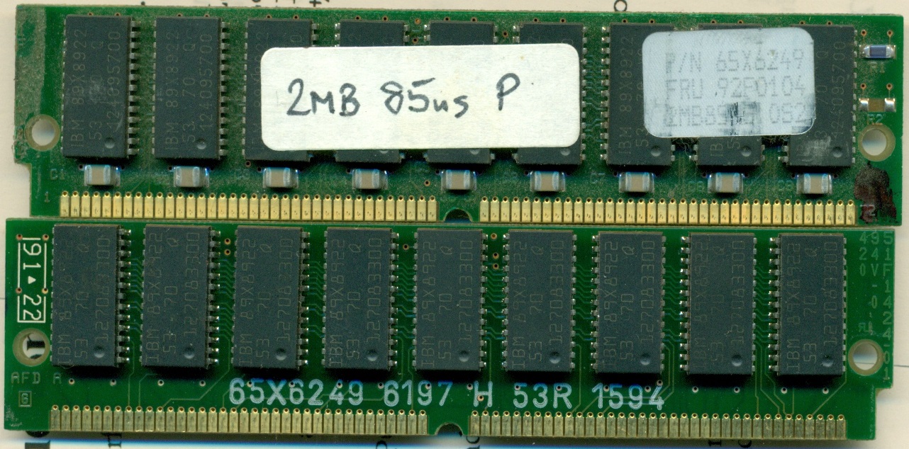 Thanks to Tim N Clarke for digging through his private stash. Notice the places for R1 and R2, yet there is no solder dots on the reverse for R3 and R4. Yet the multimeter shows OXOX (pins 67-68-69-70). From this, "masked" probably means the SIMM's PCB connects pin 68 internally, i.e. in the mask for the traces. 2MB 85nS FRU 90X8625 - P/N 65X1309 - iGH0258DA 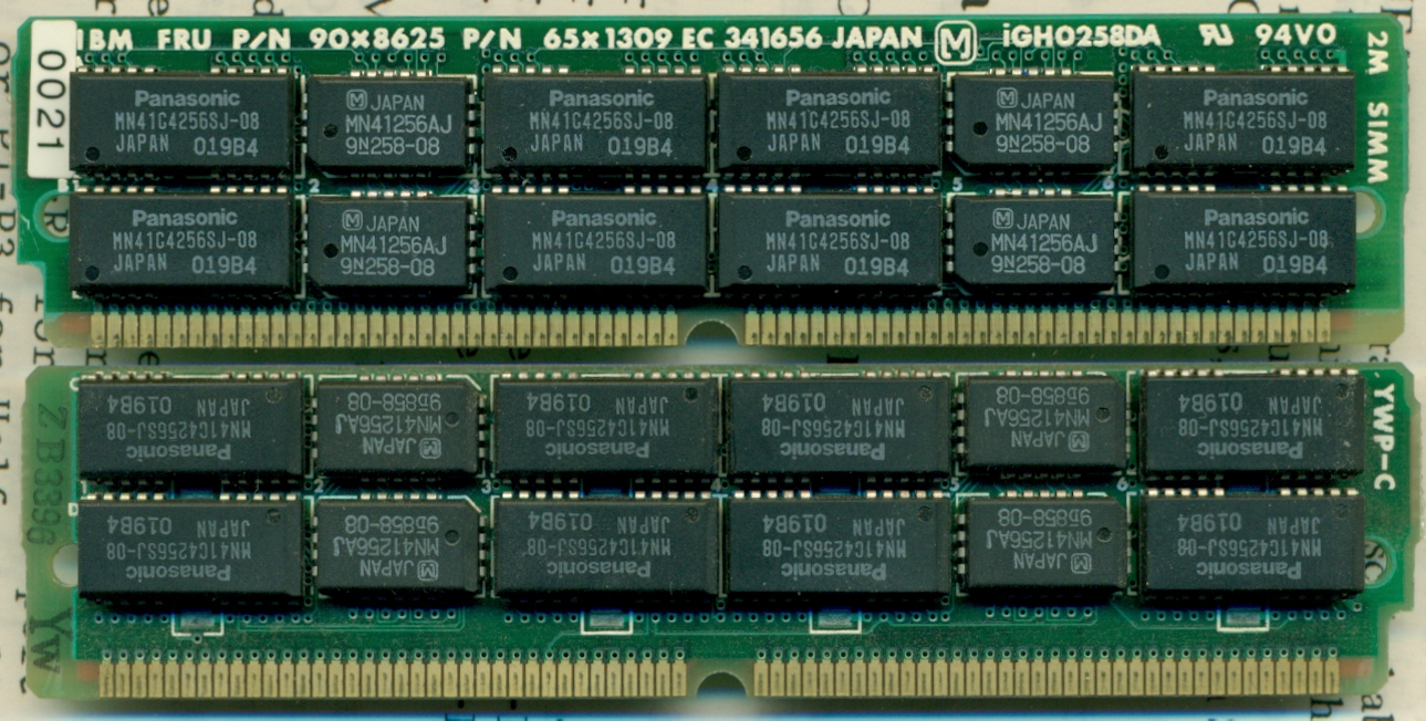 This is an original Panasonic iGH0258DA. Not even markings for PD resistors. Yet the multimeter shows OXOX (pins 67-68-69-70). PD bit shunts are definitely part of the SIMM's PCB mask. Note: the four white outlines under the big memory chips are SMD capacitors. If you look edge-wise at the SIMM against the light, you will see SMD caps under the big chips on BOTH sides.. Kingston KTM-2000/M70 Failures But whether it was all KTM-2000/M70, or M70/IBM, it
threw a 225. Peter said: P70 Old System Board FRU 65X1564 
Old System Display Card FRU 38F4686 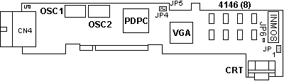
P70 New System Board FRU 56F9085 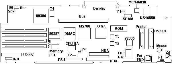
ROM is Hitachi HN27C301G-20, Datasheet Thanks to Jay P. Thorne who went through the tedious
process of pulling his P70 apart for the scans I used
for the New System Board and New System Video Card. Odd, the 8259As have been integrated into one of the
Gate Arrays. The 8042 has also been integrated, but
there is a 8042 PLCC outline to the right of the PS/2
mouse port. PRT has also disappeared. New System
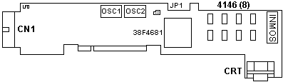
Display Card FRU 38F4686 The machine is originally a model 8573-031 (16Mhz
processor, 30MB disk), but someone has put in a 60Mb
disk. Disable ESDI Controller >I will be surprised if it can be disabled. Peter said: MCA
Bus from ESDI Port? Ed Avis replies: GRAPHICS Peter said: The VGA port supports all VGA graphics and text modes including 640 x 480 graphics, 320 x 200 graphics in 256 colors, and 720 x 400 text using any optional PS/2 VGA color display, and maintains compatibility with CGA and EGA modes. Unlike to the P75 the P70 cannot drive Plasma and external VGA at one time - except in DIAGS mode. As I said in a previous posting: the VGA chipset on the plasma-video adapter is the same 256K-IBM / INMOS stuff as used in the Mod. 50 / 60 / 70 / 80 - and therefore has the same limits: 640 x 480 at 16 colours ... ending of sending. So the answer is "No - you cannot get more colours at 640x480". I'd really tried a lot to get more out of that thing (back in the good old days) but it simply doesn't work. The available memory on the bit-planes is too low. You need at least 512K VRAM (and a better Video DAC) but the Inmos-DAC *should* be able to get it - probably. It is specified for a video bandwidth of 18.44 Mhz only (which is 640 x 480 with 60 Hz vertical refresh) - but the main problem is the missing Video-BIOS mode for 256 colours at 640 x 480 and the missing V-RAM. Simple calculation: 640 x 480 pixels =
307.200 pixels total. Each one occupies 4 bit for 16
colours = 153.600 bytes V-RAM (Video Mode 12h).
The 320 x 200 / 256-colour mode (Mode 13h) occupies 8
bit per pixel and therefore a 256-colors mode would need
double the space. I really tried to write a video driver for this thing ... but it is hard to replace hardware with software - especially if you have the hardware missing to support that. :-D >is possible to use the display card of a P/2 Model P70 in another PS/2 system with onboard VGA. I don't want to use both screens in the same time. I do not want to use any CRT. I want to use the plasma screen on my PS/2 Model 55. As far as I can tell - you can't. The
plasma board is basically a plain vanilla VGA card with
a different output stage for the row/column addressing
of a plasma display. But internally it uses the same
chips, addresses and ports like the generic onboard VGA
of the 55SX - apart from the odd form-factor of this
card. The P70 / P75 have built-in
information on this EDAF card and need no ADF then - the
55SX (and none of the "normal" PS/2 machines) hasn't. In
addition you need the P70 power supply for the high
voltages to run the plasma display. Plasma
Display Adapter Connector
Plasma Display Connector 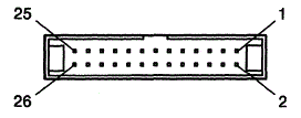 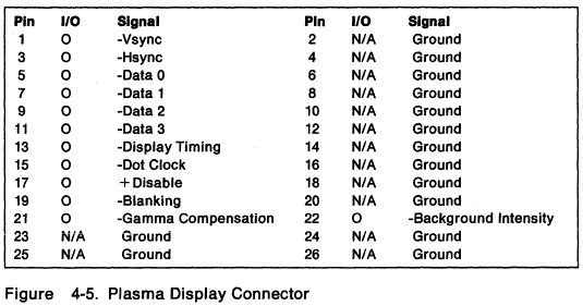 P70 Auto Dim Block Diagram Auto-dim function The plasma display has an auto-dim function. It automatically turns the plasma display off after the specified period since the last keystroke. Any keystroke returns the plasma display on. A desired value for the period can be specified approximately in the range 1 to 120 minutes during the system configuration by the backup copy of the reference diskette. Note: For German models, the background intensity of the screen is selectable. The background intensity does not affect the auto-dim function. The auto-dim logic is integrated in the PDC on the adapter card. (See Figure 4-3.) 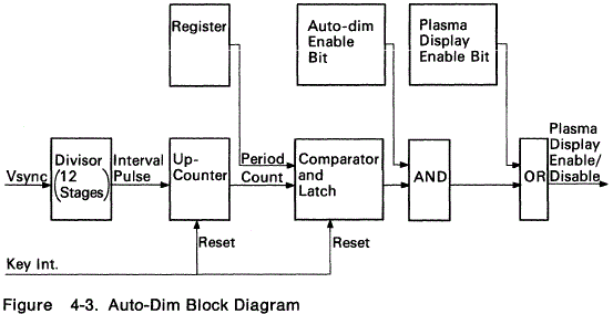 The sequence of auto-dim operation is as follows. (See Figure 4-3.) 1. During the system configuration, plasma display may be enabled (PDP ENABLE bit is set) and a value corresponding to the specified period is stored. 2. When the auto-dim function is enabled. the AUTO-DIM ENABLE bit is set by POST (Power-on Self Test). 3. The up-counter increases each minute with a interval pulse derived from the VSYNC (Vertical Synchronization) signal. 4. The comparator compares the count and the value specified for the period, then the result is latched. 5. The result is gated twice into the plasma display. If the AUTO-DIM ENABLE bit is set and the count has reached the matching value, the plasma display is disabled and the up-counter is reset. Otherwise, nothing is performed. 6. Go to step 3. P70 Plasma Pinout Arne Falch wrote: Ok, here is my first try at the pinout.: Pin: All even-numbered pins are GND. Signal connections: The connector corresponds CN1 on the drawing on your page. The machine is located elsewhere at the moment (at work), so the drawing is from memory. I will correct it if I'm wrong. The display card, left edge, where the cable to the
panel enters:
Top
of machine.
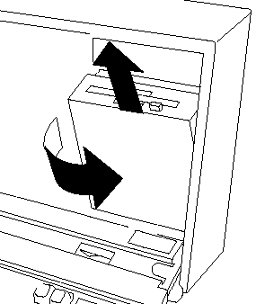
| MC edge connector Remove Floppy (H1) I have two -121s, one has the H1, the other has an H2.
Open the plasma screen so you can get your hand behind
it.Grasp the lower edge of the drive cover, pull out and
forward. Once it snaps off (you will feel it, pull the
cover up and out. If you grab onto the floppy slot, it
should give you enough of a grip to do it.
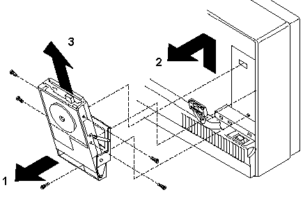
With the retaining screw loose, push the drive carrier up until it comes free of the case clips. Now you have full access to the floppy drive mounting screws.You must remove the floppy from the carrier before you can take the floppy cable out. Install Drive Carrier
ALPS DFP723D15C Rear PCB FP1T08D  The image is of the rear or bottom PCB from an ALPS DFP723D15C floppy drive, P/N 38F7802 FRU 38F5936. It is correctly oriented in the position it would be when installed, e.g. with the 34 pin header pointed down. Not a fun day. Many of the solder joints in the lower left have a "grainy" look to them. Oddly enough, the power component in the lower left corner by J4 (floppy motor power) has green corrosion on BOTH sides. One would think if it was from a leaking cap, it would be toward the source of contamination. At this point, I am hesitant to start recapping, due to the poor looking solder joints of a whole bunch of teeny tiny components. Heck, some SMD components have the grainy solder appearance looking almost as big as the component... Maybe a good application of baking soda and water could remove some of this, but I am not confident. Remove Battery 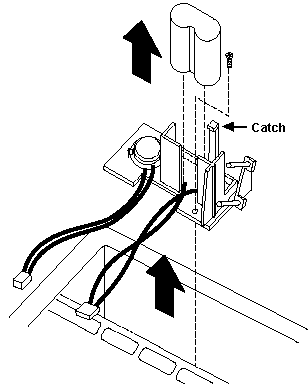
This shows how to remove the carrier and
battery. To replace just the battery, pull the catch
away from the battery, and pull the battery up. Battery
is FRU
72X8498, and the common replacements are HERE
Usually in the camera section of your local supermarket.
Pointing Device Port (or Mouse Port) Peter says: The rear port is designed 'pointing device port' in users manual as well as HMM. No keyboard will work on this port ! Don't use a serial mouse to PS/2 port adapter! You may just end up frying something! 305 error at power up
? Check continuity with a multimeter. If it reads infinite resistance it is blown. To change it: no need to remove the entire board (and too complicated anyways). Just cut the fuse with a sharp pliers directly at the fuses' case and remove it. Bend the remaining contacts up and straighten them a bit. Get a new microfuse (resistor style fuses) and solder it to these contacts. Cut off the rest of the "legs" and that was it. If the fuse was *not* blown and the machine still has a working keyboard - suspect the mouse / mouse driver to be non-functional at all. Get a "real PS/2" mouse and use the MOUSE.COM from PC/MS DOS or the MOUSE.EXE from Win95 (which is a Logitech-driver V 6.50) If you end up in a non-functional keyboard and
no blown fuse ... well ... you'd damaged the keyboard /
mouse controller, which cannot be replaced (that easy).
In this case you should try getting a replacement system
board. P70 Drive Carrier Mounting Hole Spacing 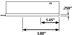
All dimensions are from the rear of the
drive. They are to the center of the hole. Be careful
when drilling! These placements DO NOT line up with the
reinforced segments of the drive case. Be careful when
tapping! Use a plug tap, a normal tap would bottom out
on the PCB. Additional features of the system unit include: o One general purpose 32-bit full-length Micro Channel slot* o Half-length Micro Channel slot o 85-watt automatic voltage-sensing power supply o Time and date clock with battery backup o Integrated 16-grayscale plasma display, integrated version of IBM Enhanced PC Keyboard. * Some half-length cards that fit in a half-length slot may not fit in a full-length slot. Auto 16/4 Token Ring Fits Lower Slot > the Auto 16/4 Token Ring fits into the bottom 16 bit slot, almost like it was built for it. Peter has a flashback and says: The Token-Ring Network Model P70 386 Adapter/A (#1598) permits attachment of the Model P70 386 (8573-061 and 8573-121) to the IBM Token-Ring Network. This adapter is half-length and designed to fit in the short slot. It transmits and receives at four million bits per second. To facilitate attachment to the IBM Personal System/2 P70 386, a unique L angle connector with a permanently attached short cable is provided. 8573-031 30 MB Hard Disk, 16 MHz planar 113 Error is a DMA timeout caused by a MCA card ... if there is nothing installed except the harddisk - replace that. It doesn't look like one, but the 72-pin card-edge connector is in fact a MCA connector (Slot 4 in the setup). > As noted in a different thread: some series of 120 and 160MB HDs did not run properly when installed "upside down" in the P70. Either they come up with a 10482 error right after start -or- fail to LLFormat / run at all later but operate fine otherwise when turned "upside up" again. (WD-3158, WD-3160). >> The -031 models used the infamous "energy conserving" harddisk, which reduced spindle speed when in idle and spins up again when accessed. A nerve killer ! > Like the Mod. 50Z and 70 the P70 had fairly lot of
problems with defunctional HDs. In the P70 *only* the
black IBM WD-series drives had been used for the 60 and
120MB models - like the WD-3158 120MB drive from the
Mod. 70-121 / -A21.
P70 Fixed Disk Drive Connector The following figure shows the signal assignment and pin numbering for the fixed disk drive connector on the adapter. The fixed disk drive connector is a 2- by 36-pin connector. Side A of the connector is the top and Side B is the bottom. Ed. HDA Upper (34 pin) and BA Lower
(40 pin). So... we have 74 pins from the headers, or so
it seems. If lucky, the Upper and Lower headers are
Signal and Ground...
Modifying 160MB SCSI Drive With ESDI
PCB The 160 operates with a different number
of sectors IIRC. Only have the data for the 80 and
160MB: 984 cylinders, 10 heads, 17 (80) and 34 (160)
sectors. So the 120 must have 26 sectors (25.5
arithmetically - but there are no half cylinders ...). I
think the 120MB controller cannot "fetch" a valid sector
start ... and therefore jumps out. The LLFORMAT routine
does not go *that* deep that it can write raw sectors on
the media. That's usually the purpose of some factory
tools.
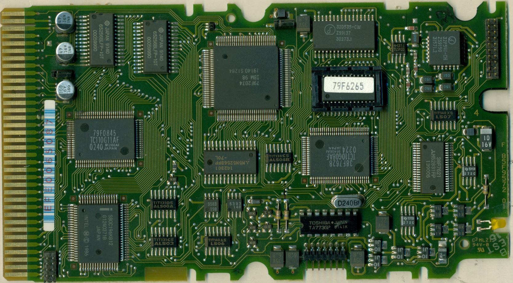
S80C31-12 Temic Semiconductors 8-Bit
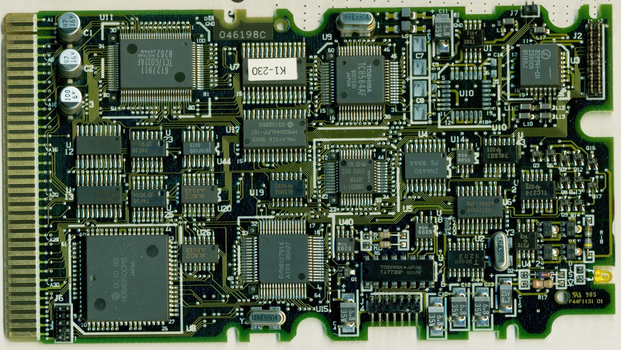
Microcontroller-Microcomputer - Programmable serial port 160MB DBA-ESDI PCB
79F6370 NO COMPONENT IDs!
79F6265 BIOS chip is a SOIC 28 like on the P75
planar... 32D535 Data Synchronizer / 2, 7 RLL ENDEC with Write Precompensation 32P541 Read Data Processor M5M5256BFP 32K word by 8-bit CMOS Static RAM 65256BLFP Hitachi TA7736P Brushless, Multi-Phase dc Motor Driver
Early
P70s Fail to Retain Configuration after Quick
"On-Off-On" >Not only the 16 MHz ones. I had this phenomenon on my 20 MHz Rev.1 (which is up and running again) also. Seems a common phenomenon for the first PS/2 - which lacked a delay in the power supply. But the early 16MHz and all Mod. 60 were pretty critical. If you didn't wait at least 20 seconds after a power down you could have wrecked the config already. |
||||||||||||||||||||||||||||||||||||||||||||||||||||||||||||||||||||||||||||||||||||||||||||||||||||||||||||||||||||||||||||||||||||||||||||||||||||||||||||||||||||||||||||||||||||||||||||||||||||||||||||||||||||||||||||||||||||||||||||||||||||||||||||||||||||||||||||||||||||||||||||||||||||||||||||||||||||||||||||||||||||||||||||||||||||||||||||||||||||||||||||||||||||||||||||||||||||||||||||||||||||||||||||||||||||||||||||||||||||||||||||||||||||||||||||||||||||||||||