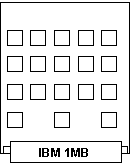
There are a few different layouts on the 1MB size. 8580 Planar
Memory Sizes
System Board 16MHz (8580-041, 071) 33F8416
1MB 80nS Memory Kit (for 33F8416) 72X6670 or 6450375
72X7475 found
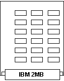
System Board 20MHz 10G4148 (8580-081, 111, 121, 161, 311,
321)
2MB 80nS Memory Kit (for 92F0756) 92F0669 or 6450379
92F0669 found. 90X7391 in Jan 1992 Pocket Ref Manual.
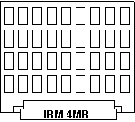
System Board 25MHz 85F0046 (8580-A21, A31, A61)
4MB 80nS Memory Kit (for 85F0046) 92F0106 or
6451060
33F5498? 34F0023 in Jan 1992 Pocket Ref Manual.
8580
System Support of Planar Memory Sizes
(From Fred Spencer, HERE)
On the initial 8580 models, only 1 MB and 2 MB planar
memory modules were available. With the announcement of
the 25MHz planars (8580-Axx), 4 MB memory cards became
available. However, it has been discovered that they
will function on the 20 MHz planars (thanks to Tim
Clarke and Joe Kovacs for this discovery). A
summary table of my experiences using various sizes of
memory cards in each of the three categories of planars
follows:
Size 16 MHz 20 MHz 25 MHz 1 MB OK
OK 225 2 MB OK
OK 225 4 MB 2 MB
OK OK
NOTE 1: 16MB planar
can use 4MB card, but can only use 2MB. [ed.]
Note 2: 225 is the
POST Error Code resulting from having memory that is too
slow.
Note 3: On some 20
MHz planars with 4 MB memory cards on the planar, the
IBM diagnostics will occasionally fail, but the memory
will still function OK. With the PIICEON 4 MB (70ns.)
memory card the IBM diagnostics may also fail. However,
both the IBM and PIICEON 4 MB memory cards will function
properly and they do pass the Norton Utilities memory
diagnostics without any problems. I will be doing more
investigation regarding this.
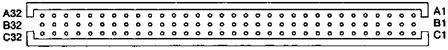
Pinout for IBM Planar Memory Cards
David Beem insinuates:
Working on the presence detect for the
Model 80 memory boards. Haven't seen the pinouts on any
pages, even Fred's, which has provided me some very good
information.
The connector is 3 rows (A, B, & C) by 32 columns.
These are marked well, except for the 2Mb board. Put it
chip-side down, connector at the bottom. The solder pads
for the connector on the circuit board now have pin A1
in the lower lefthand corner, something like this:
The Type 1, 2, and 3 system boards are equipped with two
3- by 32-pin system board memory connectors. A memory
card must be installed in connector 1 before additional
memory can be used in the channel.
The following figure shows the pin locations of the 3-
by 32-pin system board memory connectors. The pin
locations are the same for connectors 1 and 2. Connector
1 is closest to the power supply. Pin 32 is closest to
the rear of the system board.
We are mainly interested in pins A17 & A32, wired
on all Model 80 types, & pins A16 & A18, N/Cs on
the Type 1 planars, wired for the Type 2 and 3 planars.
An 'x' on the chart means the pin is tied to ground.
A16 A17
A18 A32 1Mb
x
x 2Mb
x 4Mb
x
x x
This explains why the 4Mb modules are
treated as 2Mb in a Type 1 planar. I don't know if any
of the presence detects signify memory speed. The chart
above shows the newer 2Mb board. Another surprise is the
little memory cards that go on the @FAFF.ADF 2 - 6Mb 386
Memory expansion board are the same pinouts. Of course
each board is 2Mb & the presence detect is the same
as above. I don't believe this board was offered in any
other capacity. You can use one of these little cards on
the planar, although it has to be in the slot furthest
from the power supply due to the keying &
right-angle of the connector. At least the chips are
conventional & marked as 85nS.
8580 Planar Memory Connector
Signals
-MW -Memory Write
-MA(0-8) -Memory Address (0 through 8)
-RAS(0-3) -Row Address Strobe (0 through 3)
-CAS(0-3) -Column Address Strobe (0 through 3)
-CASP -Column Address Strobe Parity
MDP(0-3) Memory Data Parity (0 through 3)
MD(0-31) Memory Data (0 through 31)
-BE(0-3) -Byte Enable (0 through 3)
R This
signal is used by POS Register 3 during system board
setup to determine the presence of a memory card in each
of the two system board memory connectors.
Note: Type 2
system board POST routines require a minimum of 1 MB of
functional memory installed in connector 1. The Type 1
system board also requires a minimum of 1MB of
functional memory; however, it may be installed in
either connector. The Type 3 system board POST routines
require 4MB of functional memory installed in connector
1.
-RAMHS
This signal is used by POS Register 4 to detect the
memory speed.
T1, T2 These
signals are used by POS Register 3 during system board
setup to determine the type of memory card installed in
each of the two Type 3 system board memory connectors.
See Section 2, "Programmable Option Select," for
additional information.
The following figure shows the pin assignments for the
Type 3 system board memory connector. Inputs (I) to and
Outputs (0) from the system board also are shown.
Pinouts: (If all pinouts could be this simple; If all
connectors wouldn't be this proprietary)
Row A
I/O
Signal
Row B
I/O
Signal
Row C
I/O
Signal
Al
N/A
Rsrvd
B1
N/A
Gnd
C1
I/O
MDO
A2
O
-MW
B2
O
+5Vdc
C2
I/O
MD1
A3
O
MA0
B3
N/A
Gnd
C3
I/O
MD2
A4
O
MA1
B4
O
+5Vdc
C4
I/O
MD3
A5
O
MA2
B5
N/A
Gnd
C5
I/O
MD4
A6
O
MA3
B6
O
+5 Vdc
C6
I/O
MD5
A7
O
MA4
B7
N/A
Gnd
C7
I/O
MD6
A8
O
MA5
B8
O
+5Vdc
C8
I/O
MD7
A9
O
MA6
B9
N/A
Gnd
C9
I/O
MD8
A10
O
MA7
B10
O
+5 Vdc
C10
I/O
MD9
A11
O
MA8
811
N/A
Gnd
C11
I/O
MD10
A12
O
-RAS0
B12
O
+5Vdc
C12
I/O
MD11
A13
O
-RAS1
B13
N/A
Gnd
C13
I/O
MD12
A14
O
-RAS2
B14
O
+5 Vdc
C14
I/O
MD13
A15
O
-RAS3
B15
N/A
Gnd
C15
I/O
MD14
A16
I
-RAMHS*
B16
O
+5 Vdc
C16
I/O
MD15
A17
I
-R
B17
N/A
Gnd
C17
I/O
MD16
A18
1
T2*
B18
O
+5 Vdc
C18
I/O
MD17
A19
O
-CAS0
B19
N/A
Gnd
C19
I/O
MD18
A20
O
-CAS1
B20
O
+5 Vdc
C20
I/O
MD19
A21
O
-CAS2
B21
N/A
Gnd
C21
I/O
MD20
A22
O
-CAS3
B22
O
+ 5 Vdc
C22
I/O
MD21
A23
I/O
MDP0
B23
N/A
Gnd
C23
I/O
MD22
A24
I/O
MDP1
B24
O
+ 5 Vdc
C24
I/O
MD23
A25
I/O
MDP2
B25
N/A
Gnd
C25
I/O
MD24
A26
I/O
MDP3
B26
O
+ 5 Vdc
C26
I/O
MD25
A27
I
-BE0
B27
N/A
Gnd
C27
I/O
MD26
A28
I
-BE1
B28
O
+5 Vdc
C28
I/O
MD27
A29
I
-BE2
B29
N/A
Gnd
C29
I/O
MD28
A30
I
-BE3
B30
O
+5 Vdc
C30
I/O
MD29
A31
I
-CASP
B31
N/A
Gnd
C31
I/O
MD30
A32
I
T1
B32
O
+ 5 Vdc
C32
I/O
MD31
Note: * Type 3 only
Peter Wendt shows a strong habit of too much time...
How about that comparison chart below ? I
once made it to build a "Mod.80-to-72pin" converter - an
attempt that failed so far, by various reasons. (Lack of
time mostly)
PIN-OUT COMPARISON CHART IBM PS/2 Mod
80
IBM
PS/2 Mod. 70 Memory Daughter
Card
72-pin
SIMM A01 NA Reserved A02 O -Memory
Write
Write Enable
O 47 A03 O -MA
0
Address
0
O
12 A04 O -MA
1
Address
1
O
13 A05 O -MA
2
Address
2
O
14 A06 O -MA
3
Address
3
O
15 A07 O -MA
4
Address
4
O
16 A08 O -MA
5
Address
5
O
17 A09 O -MA
6
Address
6
O
18 A10 O -MA
7
Address
7
O
28 A11 O -MA
8
Address
8
O
31 A12 O -RAS
0
RAS
0
O
44 A13 O -RAS
1
RAS
1
O
45 A14 O -RAS
2
RAS
2
O
34 A15 O -RAS
3
RAS
3
O
33 A16 O -RAMHS
(Type 3) 1 A17 O -R (Mod.
inst.) 2 A18 O
T2 (Type 3) 3 A19 O -CAS
0
CAS
0
O
40 A20 O -CAS
1
CAS
1
O
43 A21 O -CAS
2
CAS
2
O
41 A22 O -CAS
3
CAS
3
O
42 A23 IO -MPD
0
Parity
Data 0 IO
36 A24 IO -MPD
1
Parity
Data 1 IO
37 A25 IO -MPD
2
Parity
Data 2 IO
35 A26 IO -MPD
3
Parity
Data 3 IO
38 A27 O -BE
0
Block
Select 0 O
29 A28 O -BE
1
Block
Select 1 O
46 A29 O -BE
2
Block
Select 2 O
66 A30 O -BE
3
Block
Select 3 O
71 A31 O
-CASP
-CAS
P
O
11 A32 O T1 (Mod.
Size) 4 B01 NA
Ground
Ground
NA
1 B02 O
+5VDC
+5VDC
O
10 B03 NA
Ground
Ground
NA
39 B04 O
+5VDC
+5VDC
O
30 B05 NA
Ground
Ground
NA
72 B06 O
+5VDC
+5VDC
O
59 B07 NA Ground B08 O
+5VDC B09 NA Ground B10 O
+5VDC B11 NA Ground B12 O
+5VDC B13 NA Ground B14 O
+5VDC B15 NA Ground B16 O
+5VDC B17 NA Ground B18 O
+5VDC B19 NA Ground B20 O
+5VDC B21 NA Ground B22 O
+5VDC B23 NA Ground B24 O
+5VDC B25 NA Ground B26 O
+5VDC B27 NA Ground B28 O +5VDC B29 NA Ground B30 O
+5VDC B31 NA Ground B32 O
+5VDC C01 IO Data
00
Data
00
IO
2 C02 IO Data
01
Data
01
IO
4 C03 IO Data
02
Data
02
IO
6 C04 IO Data
03
Data
03
IO
8 C05 IO Data
04
Data
04
IO
20 C06 IO Data
05
Data
05
IO
22 C07 IO Data
06
Data
06
IO
24 C08 IO Data
07
Data
07
IO
26 C09 IO Data
08
Data
08
IO
49 C10 IO Data
09
Data
09
IO
51 C11 IO Data
10
Data
10
IO
53 C12 IO Data
11
Data
11
IO
55 C13 IO Data
12
Data
12
IO
57 C14 IO Data
13
Data
13
IO
61 C15 IO Data
14
Data
14
IO
63 C16 IO Data
15
Data
15
IO
65 C17 IO Data
16
Data
16
IO
3 C18 IO Data
17
Data
17
IO
5 C19 IO Data
18
Data
18
IO
7 C20 IO Data
19
Data
19
IO
9 C21 IO Data
20
Data
20
IO
21 C22 IO Data
21
Data
21
IO
23 C23 IO Data
22
Data
22
IO
25 C24 IO Data
23
Data
23
IO
27 C25 IO Data
24
Data
24
IO
50 C26 IO Data
25
Data
25
IO
52 C27 IO Data
26
Data
26
IO
54 C28 IO Data
27
Data
27
IO
56 C29 IO Data
28
Data
28
IO
58 C30 IO Data
29
Data
29
IO
60 C31 IO Data
30
Data
30
IO
62 C32 IO Data
31
Data
31
IO
64
Reserved
NA 19
Reserved
NA 32
Reserved
NA 48
PD
0
I
67
PD
1
I
68
PD
2
I
69
PD
3
I
70
Notes:
#1) Contact is tied to GND
if the module is High Speed (80ns)
#2) Contact is tied to GND
to signal installed module
#3) If T1=NC and T2=GND
the module is 4MB (25MHz-boards only)
#4) If T1=GND and R=GND
the module is 1MB (16MHz boards only)
If
T1=NC and R=GND there is a 2MB module installed
(20Mhz only)
T2 is
not present on 16 & 20MHz platforms and may not be
used
PS/2 Model 80 Presence
Detection - Possible Combinations +--+---+---+--------------------------------------------+ R T1 T2 Module
Presence / Type Pins +--+---+---+--------------------------------------------+ NC X X No
module present in G G
X 1MB module installed (16MHz
planar) G NC X 2MB
module installed (20MHz planar) G NC G 4MB
module installed (25MHz planar) +--+---+---+--------------------------------------------+
PS/2 Model 70 Presence
Detection - Possible Combinations
7 6 6 6 0 9 8 7 <---- Module Pins +-+-+-+-+-------------------------------------------+ 3 2 1 0 Presence Detect
Value +-+-+-+-+-------------------------------------------+ - - - - No module
present (All planars) G G - G 1 MB / 100ns Parity
(Type 1 planar only) G G G - 2 MB / 100ns Parity
(Type 1 planar only) G - - G 1 MB / 85ns
Parity (Type 1 + 2 planar) G - G - 2 MB / 85ns
Parity (Type 1 + 2 planar) - G G - 2 MB / 80ns
Parity (Type 3 + 4 planar) +---+---+---+---+-----------------------------------+ R1 R2
<----
Memory coding on original IBM-modules
Type 1 are full length 16 and 20MHz planars
Type 2 are reduced length 16 and 20MHz planars
Type 3 is the 25MHz 386 planar
Type 4 is the 25MHz 486 planar
G = GND measured against Pin 72 (module GND)
- = open connection measured against Pin 72