20181115 - This list is neither complete or totally correct. The P/N are from the 2004 version of RSinfo. The 7012-Gxx units are confusing, as are the 7015-Rxx units. I have two sources, and they don't always match when they identify planar-mount or CPU board...
I would not assume CPU cards with the same CPU are identical, unless P/Ns match.
As always, contact ME with corrections or additions.
RS6000_CPU_Cards_List_01 this table in Word 2003 format. RTF available on request.
|
Model |
ID |
CPU |
P/N |
|
7009-C10 |
48 |
80
PPC |
40H5691,
65G8331, 65G7916 |
|
7009-C20 |
90 |
120
PPC |
040H5693,
65G8126 |
|
7012-320 |
31 |
20
Pwr |
91F1009,
81F7889, 53F3352, 53F3206 |
|
7012-32H |
35 |
25
Pwr |
81F8232 |
|
7012-32E |
35 |
25
Pwr |
81F8232 |
|
7012-340 |
37 |
33
Pwr |
52G4190,
51G9539, 51G8771, 00G3149, 81F7952 |
|
7012-34H |
77 |
41
Pwr |
51G9433,
51G8989 |
|
7012-350 |
38 |
41
Pwr |
52G4007,
51G8770, 00G1998 |
|
7012-355 |
77 |
41
Pwr |
51G9433,
51G8989 |
|
7012-360 |
76 |
50
Pwr |
51G9437,
51G9074, 51G8823, 10G8819 |
|
7012-36T |
76 |
50
Pwr |
51G9437,
51G9074, 51G8823, 10G8819 |
|
7012-365 |
76 |
50
Pwr |
51G9437,
51G9074, 51G8823, 10G8819 |
|
7012-370 |
75 |
62
Pwr |
51G9441,
52G3908, 43G0914 |
|
7012-37T |
75 |
62
Pwr |
51G9441,
52G3908, 43G0914 |
|
7012-375 |
75 |
62
Pwr |
51G9441,
52G3908, 43G0914 |
|
7012-380 |
58 |
59
Pwr2 |
93H5028,
40H6723, 40H2706, 11H3465, 52G4475 |
|
7012-390 |
57 |
67
Pwr2 |
93H4897,
40H6717, 40H2837, 88G4006, 11H3462, 52G4691 |
|
7012-39H |
59 |
67
Pwr2 |
93H4924,
40H2800, 88G3536 |
|
7012-G30 |
E1D |
|
35H8750,
35H8711, 19H0229 |
|
7012-G40 |
|
|
??? |
|
7013-55L |
77 |
|
51G9433,
51G8989. |
|
7015-970 |
63 |
50
Pwr |
52G6076,
65G3448, 52G5729, 52G1072, 81F9067 |
|
7015-97B |
63 |
50
Pwr |
52G6076,
65G3448, 52G5729, 52G1072, 81F9067 |
|
7015-980 |
64 |
62.5
Pwr |
52G6085,
65G6896, 52G5669, 43G2188 |
|
7015-98B |
64 |
62.5
Pwr |
52G6085,
65G6896, 52G5669, 43G2188 |
|
7015-990 |
80 |
|
93H4848,
11H3357, 52G6128, 88G0262, 52G5755 |
|
7015-R10 |
67 |
50
Pwr |
8184780,
65G7623 * Note 1 –Rxx CPU Cards |
|
7015-R20 |
67 |
|
93H4039,
8184612 |
|
7015-R21 |
79 |
|
39H9200 |
|
7015-R24 |
82 |
71.5
P2SC |
10J2962,
40H0863, 11H7417, 88G0007 |
|
7015-R30 |
C1D |
75
601 |
35H8748,
35H8710, 19H0247 * Dual CPU |
|
7015-R3U |
C1D |
75
601 |
35H8748,
35H8710, 19H0247 * Dual CPU |
|
7015-R40 |
C4D |
112
604 |
09J4712,
19H0317 * Dual CPU |
|
7015-R4U |
C4D |
112
604 |
09J4712,
19H0317 * Dual CPU |
|
7015-R50 |
X4D |
200
604e |
Note
2 |
|
7015-R5U |
X4D |
200
604e |
Note
2 |
|
7030-3AT |
58 |
59
Pwr2 |
93H5028,
40H6723, 40H2706, 11H3465 |
|
7030-3BT |
57 |
67
Pwr2 |
93H4897,
40H6717, 40H2837, 88G4006, 11H3462, 52G4691 |
|
7030-3CT |
59 |
67
Pwr2 |
93H4924,
40H2800, 88G3536 |
Note 1:
7015-Rxx CPUs:
FRU CPU Speed
E1D PowerPC 601 75
C1D PowerPC 601 75
C4D PowerPC 604 112
E4D PowerPC 604 112
X4D PowerPC 604e 200
Note 2:
7015-R50 X4D 200 604e FRU / P/N
FRU MFG P/N
41L6222 <- 41L6221
41L5020 <- 41L5019
94H1087 <- 08L0375
08L0784 <- 08L0783
08L0373 <- 08L0372
07L8979 <- 07L8978
07L9397 <- 07L9398
94H0389 <- 93H9536
94H0389 <- 93H9535
94H0389 <- 93H9534
94H0389 <- 93H7201
The IBM RISC System/6000 processor: Hardware Overview
by H. B. Bakoglu, G. F. Grohoski, R. K. Montoye
Machine Organization of the IBM RISC System/6000 Processor
by G. F. Grohoski
Chipset Work
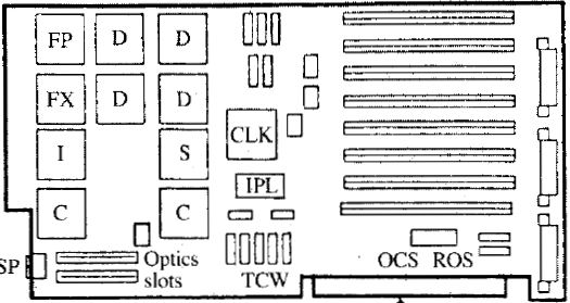
FX - Fixed Point Unit (FXU)
D - Data Cache Unit (DCU)
I - Instruction Cache Unit (ICU)
S - Storage Control Unit (SCU)
C - Input / Output Unit (IOU)
CLK - Clock
TCW - Translation Control Words (TCW) buffer
OCS - On-Card Sequencer (OCS)
ROS -
IPL -
Storage Control Unit (SCU)
The SCU is the central system controller [9]. All of the communication between CPU (ICU, FXU, DCU), main memory, and I/O is arbitrated by the SCU. The CPU sends I-cache reload, D-cache reload and D-cache storeback requests to the SCU over the PBUS, and the SCU generates the appropriate memory-control signals. The SCU is the bus master for the memory and SI0 buses. It controls the interface between D-cache and system memory, and oversees DMA operations between main memory and the I/O unit. The SCU provides a data path for I/O loads and stores between the CPU and I/O unit via the PBUS and SI0 bus. The SCU also forms an interface to the IPL ROS. Memory scrubbing is
controlled by the SCU, and memory errors detected by the DCU are recorded by the SCU. The SCU contains the bank configuration registers, which indictate the size and starting point of each bank of storage in system memory.
Cost-Reduced CPU (RIOS .9 / 8 Chip)
One of the goals of this design was to use a common chip set to produce a family of processors with varying cost and performance. This was accomplished by designing the FXU, DCU, and SCU in such a way that they can operate with two DCUs as well as with four. This system configuration is illustrated in Figure 4. Because the chips are common to the two versions, they can be sorted so that faster chips are used in the high end and slower ones in the entry-level configurations. In this way, sorting for high speed is achieved without sacrificing the overall yield.
This configuration has a lower cost for two reasons. First, it has only two data-cache chips rather than four. Second, it requires a minimum of one memory card rather than two. (This is because two DCU in the cost reduced CPU have a two-word memory interface
compared to four DCUs in the full CPU, which have a four-word interface. Consequently, some of the bit-scattering features described for the full-size CPU do not apply to the cost-reduced CPU.) To accommodate the smaller cache size and narrower memory bus width, the D-cache line size is reduced to 64 bytes. In the cost reduced CPU, fixed- and floating-point data buses are dotted together. In addition, the DCU sends the data to reload the I-cache over the SIO bus rather than having a dedicated I-cache reload bs to the ICU.