|
Rd9095a.exe Common Diagnostics for all 859x / 959x Systems 52G9619 1993 BIOS Original Mitsubishi M5M27C201 PLCC32 192-101 IBM PS/2 Enhanced 486/50 Processor Upgrade Specifications
"M"/ Upgrade 486DX 50 MHz 57F1597 FCC ID ANOIBM486B50 Sticker is 71G6207.
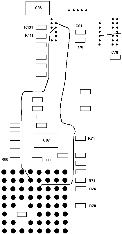
U27 BIOS.
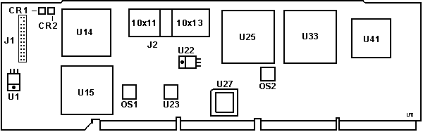
Mitsubishi variant of the 27C201, (256K x 8-bit.) J2
Header between Base and Daughter cards. 10x11 on left,
10x13 on right, 240 pins total. OS2 22.1184 MHz Osc - J1 2x13 header with one missing through hole. Earlier versions had a double pin-row connector at that place ... intended for the (or: one) predecessor of the Systems Management Adapter used on "high availability network servers". Diagnostic
LEDs Use the LEDs to help differentiate
between a processor board or a system board failure. If
you are instructed to replace one of the boards, and the
problem still exists, replace the other board (also
reinstall the first board). (Ed.
Reports coming in make me wonder about any of this. If
the board passes diagnostics, and works normally, do you
really care about the LEDs?) Enhanced
Dual Path Memory Parts
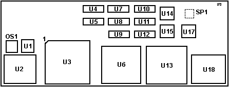
U13, U18 L2 Cache Controller Why
DX50 is on Daughtercard Ed. Also think of
the addition of the memory address buffers, which are as
big as the Memory Data Buffers. You have to shoehorn in
TWO fairly big chips, along with the discrete L2 cache,
PLUS the L2 cache controller set. Versions Incompatible with Network
Streamers The upgraded FRU with SP1 is [FRU 82G2484] should be
used with these cards. Specifications Memory
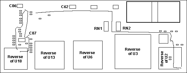
Cache: 8kb L1, 256kb L2 cache * 40 MB per second streaming data transfer support. NOTE: The M has the functional equivalence of the SynchroStream controller, but in discrete chips. The N complex is the same, where it is Streaming capable, but does not have the integrated SynchroStream chip. * Error Checking and Correcting (ECC) memory controller * 256KB Level 2 memory cache (write-through) is standard. * 20 MHz DMA; 32 bit DMA; DMA supports Subsystem Control Block. * Faster bus arbitration (than Base 1) for busmaster performance. * Enhanced Dual Path Memory * Subsystem Control Block enabled * Vital Product Data support. * Synchronous Channel Check support * Data bus parity support * A logging facility is provided (for ECC or system errors). M Complex Block Diagram 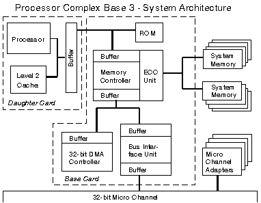 This does not agree with the actual scans of M complexi, where both the base -AND- daughter card have a pair of Memory Data Buffer / Memory Address Buffers. YMMV. Daughtercard Rework Dr. Jim sez: Documenting patch wire locations is great, but remember that there are often foil cuts associated with them. And you can't always see all of those. Ed. One can dream, can't we? I have seen one card with the older BIOS 41G9251 ('92) that has NO rework. The three DX50 I have with the new BIOS 52G9619 ('93) all have the rework. Why? Haven't a clue.
>1GB Drives as IML The M complex supports >1GB drives as the IML source. No complex BIOS upgrade is needed (or available). However, the SCSI controller needs the enhanced SCSI BIOS of 92F2244 / 92F2245 to IML properly. False
ARTIC diag error U27 Burning Rick Ekblaw plays deep safety: The M5M27C201JK is a 2 Megabit part, organized as 256K x 8, with a 12V programming voltage. Logically, it's equivalent to other 2 Megabit EPROMs in the 27-class, such as the Intel/TI/AMD/Atmel 27C020 or the Fujitsu/NEC/SGS/ST 27C2001 (see HERE, for example). However, the DIP form factor was still in common use in this time frame, and some of the PLCC varieties did not offer a windowed part (One-Time Programming only). So, the good news is that you could use
almost any 2Mb PLCC32 EPROM or PROM that you can find to
act as a replacement for the M5M27C201JK as the BIOS
chip in your M complexi (where it is only being read by
the system). For programming the EPROM/PROM, you
have to choose a part for which you have appropriate
algorithms in your programmer, because they vary. > I was all set to install a power stacker 133/586 on my dx50 in the 9595-omt. I for some reason decided to RTFM while having a cuppa. they say the powerstacker will not work with dx50. what cpu can I use to juice up the dx50.? Jim Shorney |