|
What is the complex in my 8590/95 or 9590/9595? Look HERE Crude List of Complex Capabilities Useless Trivia
OK, crankheads, here's a unscientific comparisonof some complex performances. Some unusual results.. Crude List of Complex Capabilities.
Notes:
Reason for
the Processor Complex
Complex Features
o The microprocessor
If your computer contains a processor complex, it is connected to the system board by two 164-pin, 82-position connectors, known as the processor interface connection. The processor interface connection provides: o The Micro Channel interface, which allows data to be transferred between the processor complex and the adapters in the Micro Channel expansion slots. o The system board interface, which allows the transfer of data between the processor complex and devices on the system board, such as the parallel, serial, keyboard, and auxiliary-device ports (for an explanation of these devices, see Input/Output Connectors and Ports). o Two memory interfaces (Dual Path),
systems M-Y, which the processor complex uses to read from and write to
system memory. All access to system memory is through the memory
controller in the processor complex.
L1 or Processor Cache There are two levels of cache. The cache incorporated into the main system processor is known as Level 1 (L1) cache. The 486 incorporates a single 8KB cache (Overdrive chips can have 16KB). Pentiums have two 8KB caches, one for instructions and one for data. These caches act as temporary storage places for instructions and data obtained from slower, main memory. When a system uses data, it will be likely to use it again, and getting it from an on-chip cache is much faster than getting it from main memory. L2 Cache
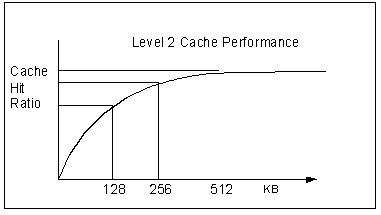
L2 cache can be accessed 5 to 10 times faster than standard memory. Cache memory uses Static Random Access Memory (SRAM) which is much faster than the Dynamic Random Access Memory (DRAM) used for system memory. SRAM is more expensive and requires more power, which is why it is not used for all memory. NOTE: The J/K/UPG 66 complexes use
17nS 256KB cache daughtercard. The UPG 50 uses a 15nS 256KB cache daughtercard.
Memory Controller The memory controller is a device on the system board or processor board that controls access to system memory by the microprocessor and I/O devices. Registers in the memory controller contain information about the amount and type of memory that is installed in the computer. During a system reset, the power-on self-test (POST) routine writes this information into the registers. (For information about POST, see Power-On Self-Test (POST) and Upgradable BIOS.) The functions of the memory controller vary among PS/2 models. They can include: o Dual-bus capability, which allows the microprocessor to read from and write to system memory while a bus master is controlling the Micro Channel bus. (See the Three Types of Overlapped Access.) o Memory timing control, which coordinates data-transfer operations involving single inline memory modules that operate at different speeds. o Cache control, which ensures the validity of the contents of the cache. The cache controller (or, in some PS/2 models, the memory controller) identifies the instructions and data that are most likely to be needed while a specific program (or part of a program) is running and copies them from system memory into the cache. During processing, as requirements change, the cache controller copies other data and instructions into the cache, replacing data and instructions that are no longer needed in the cache. Computer performance is improved each time the microprocessor finds what it needs in the cache (a cache hit). If it does not find what it needs in the cache (a cache miss), the cache controller must locate the data or instruction in system memory and copy it into the cache, while one or more wait states are imposed on the microprocessor. The cache controller manages the use of the cache so that the number of cache hits far exceeds the number of cache misses. In some PS/2 models, the microprocessor has only a built-in level-1 cache, but it supports an optional 256KB level-2 cache. This 256KB cache option increases the amount of cache memory in the computer, which increases the probability of cache hits. o Bus-width allocation, which supports 8-, 16-, and 32-bit data-transfer operations. o Memory interleaving, which is a
method of reducing the time the microprocessor has to wait for system memory
to respond during memory I/O operations.
Dual Path to Memory When bus masters were implemented on Micro Channel servers, it was found that there was often contention for memory access between the processor and the bus masters, and that the processor was being delayed waiting for bus masters to release the path into memory. The new design of the processor complexes addresses these issues by providing a dual-path into memory, effectively providing two paths to system memory, one from the processor and one from the Micro Channel. These two separate paths to system memory allow overlapping of processor and bus master cycles. (M-Y complexes) NOTE: Dual Path memory is also known as Dual Bus Interleave. Base 1 complexes also support this feature, but do not have buffers. Base 2 complexes do not support Dual Path Memory. Packet Data Transfers are used by the I/O buffer for writes to memory. This means that 16 bytes are written to memory in one processor cycle. In unbuffered systems, a write to memory is performed every four bytes. Three kinds
of overlapped cycles can occur:
Both processor and Micro Channel cycles are buffered into
16 byte blocks, further alleviating the contention for memory by reducing
the frequency of the accesses. Implementing dual-path access to memory
and the buffering of cycles can give a system throughput of up to three
times that of a server without it.
Two-Way Interleaved Memory Banks Another performance advantage is gained when the processor is accessing memory in burst mode. Memory is split into two banks, and data or code is stored sequentially across these banks; for example addresses 0 and 2 are held in bank 1, and addresses 1 and 3 are held in bank 2. The reason for this arrangement is that when a 486 burst mode request is made, the accesses to memory will be sequential. When the memory controller detects such a burst request from, for example, bank 0, it also pre-fetches the next 32 bits of data from bank 1. This way, the processor is not kept waiting while the information is being retrieved from memory. DMA Controller
When a device needs to use the Micro Channel bus to send or receive data, it competes with all the other devices that are trying to gain control of the bus. This process is known as arbitration. (For additional information, see Arbitration.) The DMA controller does not arbitrate for control of the bus; instead, the I/O device that is sending or receiving data (the DMA slave) participates in arbitration. (For additional information about slaves, refer to Slaves.) It is the DMA controller, however, that takes control of the bus when the central arbitration control point grants the DMA slave's request. DMA controllers are a dedicated unit with the ability to move data between system memory and a device on the Micro Channel. It is used by simple adapters, and also by the parallel and serial ports. Earlier versions of the Model 95 (G-L complexes) implemented a 24-bit DMA, limiting DMA memory transfers to below 16MB (whereas the 486 processor was able to address up to 4GB of memory). On 32-bit systems with more than 16MB of memory, this could cause problems if a DMA access was for memory above 16MB. The operating system could work around the problem by ensuring that DMA buffers were always below 16MB when a DMA transfer was done, but this imposes a performance penalty. Direct memory access (DMA) is a method of transferring data between system memory and I/O devices without requiring intervention by the microprocessor. DMA is more efficient than programmed I/O, in which the microprocessor reads the data from the sending device and then writes it to the receiving device. In DMA data transfers, data can bypass the microprocessor as it moves between system memory and I/O devices. DMA improves computer performance because the microprocessor does not have to interrupt its processing activities to manage data transfers. 40MBps Data Streaming
NOTE: The M and N support Streaming,
but lack a SynchroStream controller, which combines 5 chips: memory, MCA,
and DMA Controllers, FIFO buffers, and ECC logic
SynchroStream Controller 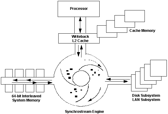
SynchroStream controllers use IBM's most advanced technology
packaging to integrate 5 major chips (memory, I/O, DMA controllers, FIFO
buffers, ECC logic) into a single chip with a RISC-like architecture. This
technology allows the high-speed interconnects and large streaming pipes
that form the SynchroStream engine to provide state-of-the-art performance.
At the heart of the computer, data is moving continually between processor, cache, main memory and the Micro Channel. Typically there is a single path to memory, so fast devices like processors have to wait for much slower I/O devices, slowing down the performance of the entire system to the speed of the slowest device. The IBM SynchroStream controller was designed to overcome this problem. It synchronizes the operation of fast and slow devices and streams data to these devices to ensure all devices work at their data at their optimum levels of performance. Synchrostream is an intelligent device in that it predicts
what data the devices will need and loads it from memory before it is requested.
When the device wants the data, it is presented to it from the IBM SynchroStream
controller and the device can continue working immediately, as it does
not have to wait for the data to be collected from memory. When devices
are moving data into memory, the IBM SynchroStream controller holds the
data, and writes it to memory when it is most efficient to do so. Since
devices are not moving data to and from memory directly, but to the SynchroStream
controller, each device has its own logical path to memory. Devices do
not have to wait for other slower devices.
The IBM SynchroStream controller is located on Pentium
processor complexes, in the Server 95 and Server 95 Array systems. Implementation
on the processor complex means that current PS/2 Server 95 and PS/2 Model
90 users can easily upgrade their machines to have IBM SynchroStream controller
functions.
Key advantages
of the SynchroStream
16 Bit Busmasters
Complexes
work in all 8590 / 8595 / 9590 / 9595 / 500
NOTE: The power supply in the Model 90 case is supposedly a little small for the DX50, P60, P66, and P90 complexes. And in addition, the air baffle in the Model 90 may have to be removed if a processor with a big heat sink or heatsink / fan combination is installed. BUT I have to wonder- it's rated for 215 Watts, it isn't THAT small..Hell, the 9577 PS is only 194 Watts. 95A Planar Lacks Backward Compatability
More Useless Trivia
Obviously not only the speed ...
Mentions "optional 256K cache" - which makes clear that no other board than 64F0198 and 64F0210 is meant. The 486DX2-33/66 board 92F0145 is then a much later developement out of the Non-SOD 64F0198 - intended to use Flash-BIOS, but not fully developed or supported. (That's the board with the odd bank-select jumper in the top/right corner) (Ed. edit based on personal inspection of a 92F0048) The 92F0048 appears to be also based on the Non-SOD 64F0198, with a DX50 cpu, a 50MHz oscillator, and some decoding circuitry mounted in the area that on the SOD would go on. The matching 12nS cache module is 92F0050. The smaller type-1 platforms had been offered to form "entry models" - focussed on the Mod. 90 (92F0065 - 486SX-20 and 92F0049 - 486DX-20). The 92F0065, which I call "Kiddies CPUs", is the only one which has a 487SX-presence" Jumper. A totally different thread are the Type-2 platforms, which all base on the 92F0079. The type-2 platforms have been developed to make memory selection a bit easier - for the cost of some performance as a cost-efficient solution. The type-3 platform of the -M- class has been intended for high-end servers: paired memory *and* ECC support. Only few Mod. 90 saw this platform as far as I know. Don't know if IBM ever offered it officially in the 90. I remember having seen 2 or 3 Mod. 9590-AMF at a customer - but they had the [PA]-sticker close to the Serial-number decal ... which identifies them as "upgraded machines". The -M- platform even survived the change from the 8595 to the 9595 (with the old planar and LED-planel however) along with the 92F0161 486DX2-25/50 -L- platform. Strange enough. The final stage of the 486-line was reached with the Type-4 -N- class board 61G2343 - which was the precessor to the 5V-Pentium (P5) platform. This however is a totally new developement, at a time when 486 processors were already a bit dusted. The Type-4 platforms are all very similar with the integrated
Intel Cache chipset. I think there has been a lot experience used from
the -M- class DX-50 board. But this time everything fits on *one* printboard
and make the funny shielded hi-density connectors obsolete for the "second
>Are there any ECAs related to any specific FRUs?
Unsorted Oorts
Can't See >16MB Under W95 HIMEMUPD.EXE is the cure On an IBM PS/2 Model 77, 90 or 95 computer with more than 16 MB of memory (RAM) installed, Windows 95 only recognizes and uses 16 MB of memory. This is because HIMEM.SYS, the extended memory manager, only detects 16 MB of memory installed. CAUSE These computers use a nonstandard API for reporting memory in excess of 16 MB that is not supported by Windows 95. RESOLUTION This issue is resolved
by the following updated file(s) for Windows 95 and OSR2, and later versions
of these file(s): HIMEM.SYS ver 3.95 dated 10/2/95 33,127
bytes
STATUS Microsoft has
confirmed this to be a problem in Microsoft Windows 95. An update to address
this problem is now available, but is not fully regression tested and should
be applied only to computers experiencing this specific problem. Unless
you are severely impacted by this specific problem, Microsoft does notrecommend
implementing this update at this time. Contact Microsoft Technical Support
for additional information about the availability of this update.
MORE INFORMATION The computers listed in this article use INT 15 ax=c700h to report memory above 16 MB. (Other IBM PS/2 Microchannel computers may use INT 15 ax=E881.) The updated version of Himem.sys accepts a /P switch that causes HIMEM to use this API to detect memory in excess of 16 MB. Without the /P switch, the updated HIMEM does not use this API, and functions the same as the shipping version of HIMEM. The new version of Himem.sys reports itself as version 3.95,
the same as the shipping version. Knowledge Base Reference Article: Q137755:
No More Than 16 MB of Memory Reported on IBM PS/2 Model 77, 90
|