|
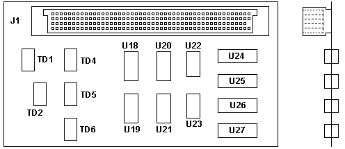
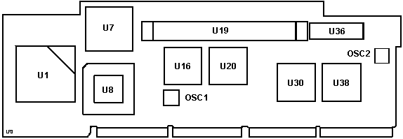
rd9095a Diagnostics (common to all T1-4) Type 1 BIOS Images 84F9154 SOD Type 1 with socket -OR- solder pads for Weitek 4167 84F9155 Type 1 "J" and "K" with Weitek socket 91F9812 Non-SOD Type 1 with nothing but SMDs or resist to right of CPU. 52G9509 "8590/95 Dual Booting Capability EPROM" EPROM for all Type 1 [except T1 486DX2-66 Upgrade] AM27C010-155DC 1 Megabit (131,072 x 8-Bit) CMOS EPROM 32 pin, .600 spacing EEPROM for T1 486DX2-66 Upgrade AM28F010-150JC 1 Megabit (128 K x 8-Bit) CMOS 12.0 Volt, Bulk Erase Flash Memory SCSIFIX.ZIP Finally! A utility to alter the number of sectors for a SCSI drive and convert them to a 3.94GB drive! Bob Eager, you have answered a prayer! Specifications Memory supported, cache, features 256K Cache Daughtercard for Type 1 L2 Cache Option Variants -17nS and -15nS L2 Cache Performance ODP vs. ODPR Complex BIOS Upgrade Needed for >1GB IML Drive Upgrade EPROM Additional Capabilities Complex EPROM Speeds Type 1 Complexi Upgrade to "8590/95 Dual Booting Capability EPROM" "G" 486SX 20 MHz "G" Processor Upgrade "J" 486DX 25 MHz 64F0201 CR1 What? Tracking 4167 Capable Complexi Info on Weitek 4167 "K" 486DX 33 MHz 64F0198 What is the Square Of Death? Square of Death Limits ECA 0530 0Kx complexes with Complex P/N 84F9356 Upgrade 486DX2 66/33 92F0145 Supports Non-IML! Upgrade 486DX 50 MHz 92F0048 Identify Upgrade 486/50 Common Features of the Type1 20MHz DMA and MCA Bus interface. Socket for 256K L2 Cache daughtercard (except "G" complex) Memory controller can access up to 64MB of planar memory DMA controller originally limited to 16MB. Fixed by the last BIOS update (unknown how) Memory controller supports parity, matched SIMMs only.
"G" 486SX 20 MHz 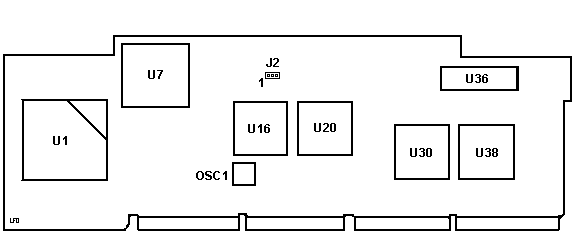
On the 20-MHz board, jumper 2 must be on 1
and 2 if a 487SX processor is installed in position U1 .
If there isn't a 487SX in U1 , the jumper must be on 2
and 3. NOTE: When
installing a CPU, align beveled corner with the beveled
outline on the board. NOTE: The "G" is
the only Type 1 complex to lack a 160 pin L2 Cache
option connector. 256 KB
Cache Memory Option Kit, 17nS and
15nS [Work in Progress!]
4 KB
of "TAG SRAM" stores some of the cache item's
address bits, used to store and locate the item,
and some bits used for validity checking. "Cache Controller" coordinates access to the SRAM. On a cache-hit, the controller organizes the access of the data from the data SRAM using the TAG SRAM address. On a cache-miss, the controller places the new data into the cache, updating the TAG SRAM and data SRAM at the correct index location.
Optional Cache Card Installation Plug the 256 KB cache onto the receptacle on the complex. One pin, called the "key", has been removed to provide a guide for inserting the card correctly. 256K Cache Not Visible
under System programs? L2 Cache Option Variants 256K 17nS Cache Daughtercard 6451095 (64F0199 same thing) 64F0199, Back Side
Bitsaver [pages 417-422] Fil-Mag or Sprague 77Z14Annn Active TTL Delay Module Equivalent to bel S423-00nn Active TTL Delay Module 64F0199, Front Side
TI SN74ACT2160-17FM 8K x 4 2-Way Cache Address Comparator/Data RAM Bitsaver physical pages 170-194 Ed. The chips
change from module to module. Yours may be different. I
see no specific memory or cache controller chips [yet],
the AMD chips are GAL/PALs, and they probably aren't the
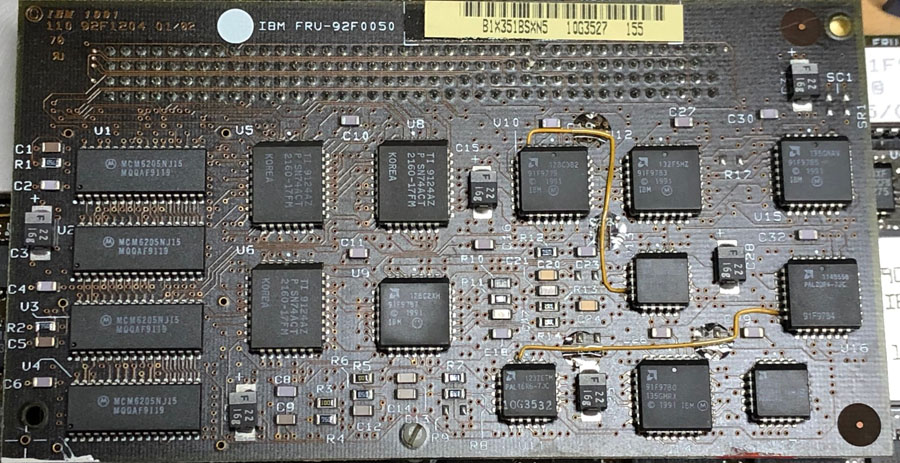
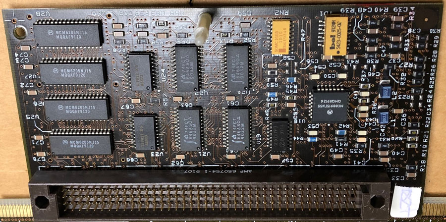
highest performance option... 92F0050 / 10G3527 Front Side
Thx to Lorenzo Mollicone Huh, U11 is 10G3532. P/N is 10G3527. All the other
PLCCs are 91F97nn. 92F0050 / 10G3527 Back Side
Thx to Lorenzo Mollicone Significant change from -17nS version. The 64F0199 uses
five Fil-Mag Delay Modules and the -15nS uses ONE bel
S423-0025-02 . bel S423-0025-02 5
Tap Leading Edge Control Standard Delay Module HERE
Motorola
MC88915FN55 Low Skew CMOS PLL Clock Driver 55MHZ
28-PLCC How Does System Know That
Cache Installed if it Doesn't show Up?
On -17, U11 is 84F8257, different from most of the
PLCCs. If I could see a sticker on the 64F0199, I bet it
would be 84F82nn... Example Multi-Card Adapter is the Image
Adapter/A I'm not so sure that the L2 cache module has a "POSID" as such, but as you speculated, some of the ID pins on the interconnect are tested to "modify" the complex's configuration table during POST.
L2
Cache Performance From Tony Ingenoso From Charles Lasitter From Tony I don't see this as a core multiplier
issue -- even the low end DX25 T2 runs better than one
might expect it to. The kernel rebuild improvements
aren't surprising - compilation algorithms and the bits
of data they work tend to be well localized if modules
aren't too massive. Initial parsing would be very
read intensive as well and should make good use of an
L2. Cache performance is indeed a very task specific
kind of thing. Scattered code/data can effectively
neutralize it totally. DX50's are strange -- they often outrun DX2-66 when main memory bandwidth or I/O is the constraint. When staying in L1, then the DX2-66 wins due to the multiplier. With a fast L2 and fairly scattered code/data a DX50 is going to do very well. From Peter The 486DX2-33/66 showed 33 BogoMips, the
DX50 25 only ... same as the T3 DX50 while a DX2-50/100
(Intel DX4-100 in 2x mode) on a T3-platform runs at
-supposed- 50 Bogomips almost. In the practical use the T1 DX50 wasn't
much slower than the T1 DX2 - the XF86 stuff paced at
the same rate on both. None of the machines "felt"
faster or slower. The DX4 T3 was a bit faster - but not
significantly. All 3 machines had the same XGA-2 card,
the same TR 16/4 network adapter, the same 32MB Parity
RAM and the same IBM 400MB HD with the Linux on it. The T1 platforms had the "plug on" 256K
L2 cache (17ns on DX2, 15ns on DX50) and the T3 had its
own integrated cache. I did not write down all the
values ... maybe I should repeat that session again to
get some definite, comparable data. ODP vs. ODPR 169 pin ODP - 487SX installed with 486SX still in place, needs the "SX-disable" pin. Important on boards with soldered CPU. 168 pin ODPR - (R - "Replace") replaces 486SX / 486DX does not need "SX-disable" pin. Complex BIOS Upgrade Needed for
>1GB IML Drive This same feature is related to the IBM
controller's inability to do an actual format of the
drive if there has been an IML partition on the drive
before. The space at the end of the drive is never
released, because the IBM controller refuses for format
that area of the drive. That's why I typically use the RAID
adapter when I REALLY want to nuke some drives. Upgrade
EPROM Additional Capabilities
Complex
EPROM Speeds Peter replies: Type 1
Complexi Upgrade to "8590/95 Dual Booting Capability
EPROM" PROCESSOR FRU P/N
MODEL EPROM
P/N
LOC. PART NUMBER 52G9509 (was 52G9750 - try this if other PN is not known) NOTE: Use
the latest refdisk and diags. See above... "J" 486DX 25 MHz 64F0201 (old 84F8036) ANOIBM486A25 191-052 IBM PS/2 486/25 AND 486/33 PROCESSOR UPGRADE OPTIONS 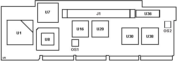
J1 The 160 position connector is AMP 650756-1, dtd 9145. J8 was a socket for the 4167 Weitek co-processor. The "J" complex has three guises: J8 present: 142 pin socket for Weitek 4167 J8 absent: Solder pads, no socket SOD - likely will NOT support 5x86 J8 absent: No solder pads Non-SOD - Likely supports 5x86 CR1 What? 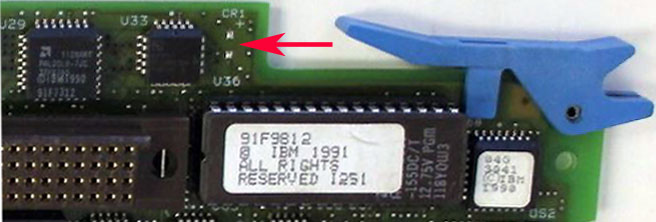 You can see this on a number of Type 1 complexi, including the Upgrade 486DX2-66 and the Upgrade 486DX-50. What is CR1 for? Tracking 4167 Capable Complexi Looking into the functionality of a Weitek 4167 "Abacus" in the U8 position. From this VERY limited sample, it seems you need 54F2958 Memory Data Buffer (old) in U16, 20, and 30 to support the Weitek 4167. Special J (J with 4167 socket) PCB 84F8036 026 Small sticker on Weitek socket "Kit 34" Complex BIOS "IBM Confidential" U2IT16 84F9155 18 June 90 54F2958 Memory Data Buffer (old) 57F2194 Memory Controller Not So Special J (4167 socket) Lorenzo Mollicone sent some pix, 84F8208 (handwritten on sticker) BIOS 64F6032, 1990 54F2958 Memory Data Buffer (old) Info on Weitek 4167 Weitek Abacus FPU by Axel Muhr WeitekDisk.zip Test suite from Weitek Applications that took advantage of the Weitek Abacus were scarce. AutoShade, Autodesk Renderman, 3-D Studio were the most prominent to use a Weitek coprocessor. If you happen to own one, you might actually use or at least test it… so here’s the official test-suite from Weitek. If contains these toolsDOS TSR to update the BIOS for Abacus support (if missing) Test tool - checks for Abacus presence using INT 11h BIOS calls. Diagnostic tool 2 demos: Side-by-side Mandelbrot benchmark and rendering Phong shaded beach ball Abacus macros for using it natively in your cool assembly code copro16a.txt The best source of technical information about the 4167 is the highly recommended copro16a.txt by Norbert Juffa in 1994. 4167 Floating-Point Coprocessor advanced data 190-186 IBM PERSONAL SYSTEM/2
486/33 PROCESSOR UPGRADE OPTION
The K complex has been seen in three guises: "Special K" (American breakfast cereal) Non-SOD Ks (Nothing where U8 was, just green resist) What
is the SOD? David Beem responds: >Regarding the sensitivity of this complex, has anyone ever tried to swap the BIOS with another Type 1 complex that is known to work with the faster CPUs? Despite the complexi being
very similar & using the same reference disk,
fundamental changes for things like the Weitek
coprocessor could really mess things up. IBM would issue
a whole complex if there was problems, not just a BIOS
change. Other than the T4 'N' I have seen no evidence of
other complex types checking things like CPUID. SOD
Limitations from Tim Clarke Not having a SOD Type-2 I can't test this, but I would expect the same limits to apply. So, you should be able to run a DX2-50, DX2-ODPR (@ 50Mhz), Cyrix/IBM 5x86 (@50Mhz) or AMD 586 (@ 75Mhz) in a SOD Type-2. The 'performance' of a Cyrix/IBM 5x86 @ 'x2 clocking' and the AMD 586 @ 'x3 clocking' are *roughly* equal, although I have a preference for the Cyrix/IBM chip. ECA #0530 90-0K9/95-0KD with Complex P/N 84F9356 Steven Wachtel wrote: These systems appear to have a memory
management problem. In my environment it was seen on a
Model 90 with 16 MB of RAM. The system would hang during
OS2 boot or during invocation of simple processes after
a basic install (such as the system editor ). Symptoms
at other OS2 sites would include excessive "random" trap
errors. Not using DOS on these systems, I would expect
the problem to surface as some indeterminate memory
related failure in the E/XMS region. During initial setup of this
machine, the problem appeared as an inability to create
a usable backup reference disk ( if said disk was used
there were always errors ). On restart after the
failure the machine will request to exec its own
auto-reconfiguration and mark out the "bad"
regions. For my situation I had the IBM CE on-site
for ~6 days for two separate events. The CE
changed each memory chip and riser (for the M90)
multiple times and recombined them in every combination
representation. Today (11/5/91) after following his instincts and direction of the higher level support reps, he contacted them again. They asked for the part number of the CPU board, upon which rests a Gate Array based custom memory controller. He was advised that there are *known* problems with the down-rev boards in my new machines. This problem exists(ed?) on the 0KD models of the M90 and M95, and possibly (as I do not have any to verify this ) the 0JD models. IBM's second level support is apparently aware of this potential problem, but has not disseminated this to the CE level or the purchasing customer. Problem part identification
and rectification: Upgrade 486DX2-66 92F0145 / 52G9480 / ANOIBMB33 192-178 IBM PS/2 486DX2-66 PROCESSOR UPGRADE OPTION 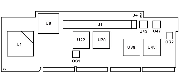
J4- Once you toggle
this jumper you will end up in a 0129 3000 error -
"EEprom Jumper is in the wrong position" and no boot or
such. I'd reported that some time ago while testing
around with the 92F0145. NOTE: Leave J4
jumper on the center and bottom pin, "R" Peter sez: But the system permanently fails to boot
into this Type 1 reference partition. Once you reboot it
and press [ctrl]+[alt]+[ins] at CP 66 (cursor top /
right) the machine loads the operating system instead
jumping into reference. The platform nicely takes the Kingston Turbochip *without* restoration of the system partition. Runs fine with it - right from the start. Supports
Non-IML Configurations His guess was this complex was designed
to support RAID Arrays, and the early RAID controller,
"Passplay" had no ability to boot from an array. Upgrade 486DX 50 MHz 92F0048 191-096 Personal System/2
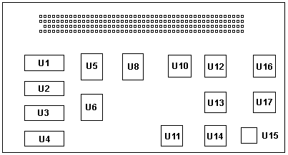
486/50 Processor Upgrade Option [Type 1 486/50] Peter We, the god-Emperor- As surmised before, the T1-50 "Big 50" was released to allow 486DX-50 power without ECC support without the need for the double-deck M. I'm not so sure that is the case... 191-198 IBM PS/2 486SX/25,33,50 PROCESSOR UPGRADE OPTIONS Oct 17, 1991 192-101 IBM PS/2 ENHANCED 486/50 PROCESSOR UPGRADE OPTION Apr 28, 1992 Here is my SWAG... Get your Dr Dentons with footies out of the oven, put 'em on, grab a piping hot mug of mint truffle cocoa, and pile onto the sofa.... IBM introduced the G, J, and K in Oct 90. Supposedly. The T1-50 was released in Jun 1991. This might have been due in some measure to the initially low yield rates for the Intel 486DX-50. So far, there is no SOD version of the T1-50, which suggests the T1-50 is similar to the non-SOD K. This is where we will never know. My guess is the T1-50 was perhaps memory or I/O bound as compared to the M. The M adds buffering on both address and data lines [IIRC]. But adding another buffer on a T1 complex would run into a problem of physical space. Peter points out the distance limits between the 486DX-50 cache controller chipset, the L2 cache, and the CPU. IBM juggled things around and loaded up the daughtercard... So in the efforts to correct the first issue, IBM was dumped into a whole 'nother conundrum... To be klar about the improvement in the M complex: Enhanced dual path memory design (Dual Bus Interleave). Although Base 1 allows both the processor and busmasters to access memory concurrently through two paths, the Base 3 and 4 has buffers at both paths to provide better performance. Also the buffer on the adapter side (I/O buffer) uses packet data transfers for writes. This means 16 bytes are collected and this packet is written in one cycle to memory as opposed to writing for every 4 bytes received (as with unbuffered systems). Lorenzo Mollicone The Announcement Letter says "... an external 256KB level two cache is provided as standard on the processor complex" All of my boxed Upgrade 486DX-50 Processor Upgrade Options have the L2 Cache. Upgrade 486DX 50 MHz 92F0048 [Updated thx to Lorenzo Mollicone] 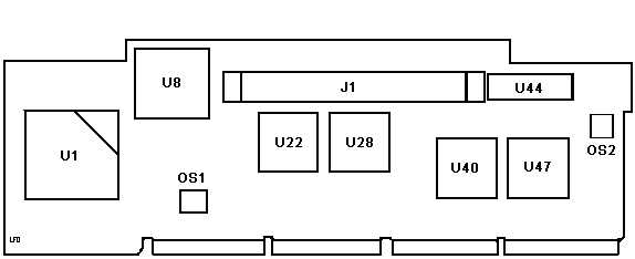
U44 Complex BIOS
Stock version is 91F9812. This version does not fully
support the F/W SCSI [Corvette] and IML from up to
3.94GB drives. To get the most out of this complex, you need the 52G9509 "8590/95 Dual Booting
Capability EPROM" -AND- the SCSI adapter needs the 92F2244 and 92F2245 SCSI BIOS
Firmware. All three can
Spocks, short
Tribbles, and all Fast/Wide SCSI
adapters come stock with the 44/45 SCSI BIOS pair. Some observations- The Upgrade 486DX-50 is a Type 1 with true 50MHz CPU on
the complex! All Type 1 complexi [except "G"] use
a 160 position 4x40 receptacle for the L2 Cache option.
Having the 486DX-50 on the complex PCB instead of a
daughtercard means that any upgrade CPU will NOT be
getting close to a Model 90 memory riser! NOTE: On the
Upgrade 486DX-50, the CPU clock, OSC1, has been moved
from being under the left side of U16. It is visible
even with an L2 Cache option installed. OSC1 is a black
SMD, so if you don't see a shiny oscillator like you are
used to, look again. NOTE: The Type 3
"M" complex is the only other true 486DX-50, but the
"M"'s DX-50 is on the daughtercard! [M is also called
the "double-decker"] NOTE: The Type 3
"M" complex is the "Enhanced 486/50" while the Type 1
486/50 is the "486/50 Processor Upgrade" 192-101 IBM PS/2 Enhanced 486/50 Processor Upgrade Option Double-deck "M" for upgrading an existing system. IBM included a tiny "P3" sticker. FCC ID- ANOIBM486A50  To positively identify the Upgrade 486/50, look at the
back for the FCC ID sticker. I have noticed that
sometimes, an older complex that was replaced is put
into the box from the upgrade. 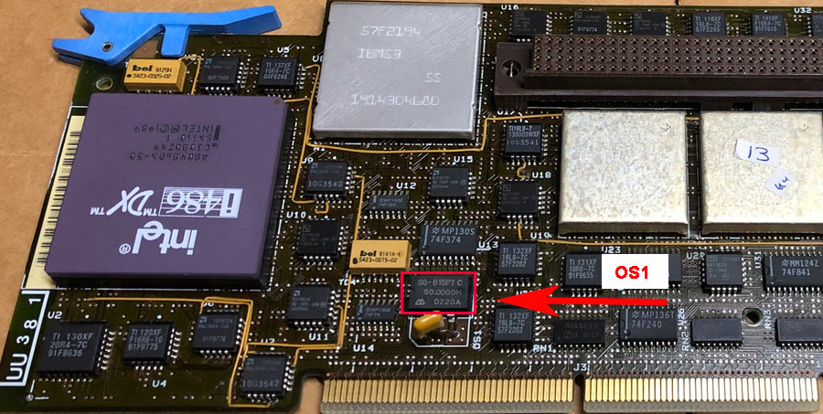 What happens: A 486/33 "K" is replaced by a 486/50, the "K" is put into the box, and through no fault [it is almost 30 years old!] the complex is called a 486/50 because that's what is on the box... This happens with other adapters as well. The 486/50 is easy to identify, the location of OS1 is to the left of other Type 1 complexes, OS1 is 50.0000 MHz, and OS1 is an SMD [black plastic]. All other Type 1 complex use metal canned oscillators. NOTE: The yellow component just below OS1 is "A5C 334K". So if you want the fastest Type 1 complex, remember that Black is Beautiful! Specifications Memory, Cache, Features Min/Max on system board: 8/64MB RAM: PS/2 FPM 72-pin SIMM. Interleaved (Install SIMMs in pairs) 70ns parity checked 80 and 85 (ns) memory Single In-Line Memory Modules (SIMMs) are supported, 70ns memory SIMMs provide optimum memory performance. ROM: 128KB * Socket for 17nS L2 256K write-through L2 cache on "J", "K", and "Upgrade DX2-66" * Socket for L2 256K write-through L2 cache on "Upgrade 486DX-50". * No Weitek 4167 coprocessor socket on later "J", "K", and "Upgrade" complexes. * 24 bit DMA; 10-12 MHz. (10-12? One or the other, please) * Dual path memory design (Dual Bus Interleave). * 20 MB per second data transfer support (for MCA bus) |