|
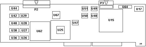
Trademark Info "sabine" or "High Performance 3D Color Graphics Processor".devices.mca.8ee6 IrisVision Cards IRISVision General Components 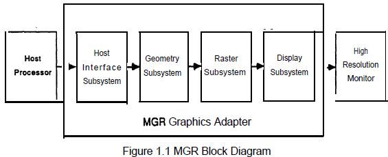 MGE2 Base Card (Card has both GE and HI) The Host Interface subsystem interfaces to the host processor via the Micro Channel Architecture (MCA) bus. It provides all of the necessary data and control signals required by the MCA bus. It also interfaces to the other three subsystems over a local bus which is compatible with the SGI private bus. The Host Interface Subsystem provides the programmable Option Select (POS) registers which are used to configure the MCA bus interface aspects of the adapter. MGE2 Geometry Engine Subsystem The Geometry subsystem contains the Geometry Engine which is used to perform the geometric transformations and lighting calculations on the graphics data. It also performs the clipping and high level rendering calculations before sending the data to the Raster subsystem. The Geometry Engine performs high speed floating point calculations under the control of the onboard microcode. MGE2 Host System Interface The host system issues commands to the Geometry Engine by sending command tokens and data parameters down a FIFO. The Geometry Engine reads the FIFO and performs the desired functions. The Geometry Subsystem also contains hardware which controls the addressing of the hardware components in the Raster and Display Subsystems. MGE2 Base Card FRU: 42F6842
XL-3132 Floating Point Processor Datasheet This is the
MicroChannel Geometry Engine. It is based upon the HQ
integer processor from SGI (rated at 10 MIPS) and the
Weitek XL-3132 floating point processor (rated at 20
MFLOPS). The geometry engine provides the host
interface, handles DMA operations, and handles all the
matrix operations, lighting and coordinate
transformations. 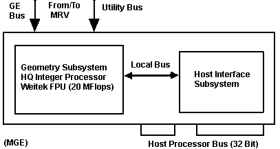 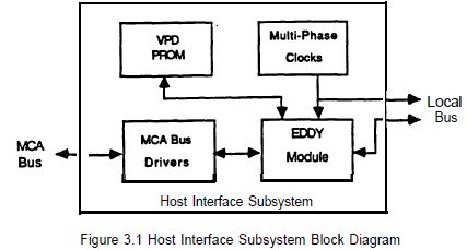 GRFl
Gate Array EDDY
Module (U15?) The Eddy module only responds to 32-bit Masters when operating as a Memory Slave device. All data transfers to the local bus are 32-bit transfers. The Bus Master DMA feature of the Eddy module will always perform a 32-bit transfer and therefore should always be programmed to transfer data to or from system memory (i.e. 32-bit Slave Memory). The following paragraphs describe the address decoding performed by the Eddy Module. The Eddy module provides a bus
translation from the MCA bus to the Local Bus, Address
Decode Section: responsible for control
of read and write operations to POS Programmable
Option Select (POS) registers contain
information to identify and configure the adapter,s
eliminating the need for hardware jumpers. There are
eight directly addressable 8 bit POS registers, as
shown in Figure 3.3. Four sub-data registers are
accessible through the use of a sub-addressing
facility. One of the POS registers indicates channel
check status information which is only valid is after
an error has caused the Eddy module to Channel Check
the host system. NOTE:
I want to illustrate the options. POS and Bit numbers
omitted at random. - Interrupt Request (IRQ) Level - Card enable/disable bit - Byte Order Selection bit - Wait State Selection bit - DMA block transfer size and DMA Bus Master enable/disable bit - Data Streaming Mode enable/disable bit - Error checking enable/disable bits . - Memory address - Arbitration Level - Fairness enable/disable bit - Channel Check Status - VPD subaddress registers NOTE: Channel Check Status / Sub-Address Register (POS 6) has two functions which are controlled by the status bit (bit 6) of the POS 5 register. If the status bit is 1, this register is defined as a sub-address register. If the status bit is a 0, this register contains status information about the pending Channel Check. Remember the RS/6000 9-K 10/100 bit Ethernet? It has that PCI to MCA bridge chip (ASIC by AMD) and a bog standard PCI Fast Ethernet controller. Speculation is that XPOS are used to access the PCI Ethernet chip, but we would need to dump the ODT for it in order to find out... Control
/ Status Section contains the seven
32-bit registers as shown in Figure 3.4. Some of the
32 bit registers are accessible as multiple 8 or 16
bit registers. The byte ordering of the host machine
will affect the address required for accessing the
registers when accessing 8 or 16 bit portions of the
32 bit registers. These registers are defined in the
registers The Eddy module contains two DMA
channels. Each channel will arbitrate for the Micro
Channel on the same arbitration level. These channels
will operate in a serial manner so that a transfer on
one channel will complete before a transfer on the
other channel can begin. If an error occurs during a
DMA transfer, that transfer will be terminated. The
other channel will not be able to begin a transfer
until the one that was terminated is allowed to
complete. VPD PROM NOTE:
Thank SGI, each VPD chip is socketed into individual
pin sockets! Multi-Phase
Clocks Section MCA Bus
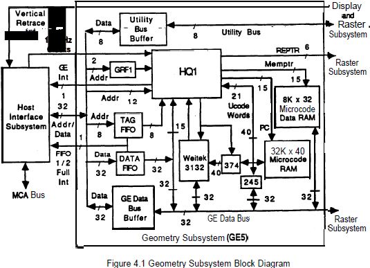
Drivers Geometry
Subsystem The HQ1 chip controls address
decoding for host and acts as a microcode sequencer.
The Weitek 3132 chip performs floating point
calculations and is controlled by HQ1. The microcode
RAM holds the microcode, while the microcode data RAM
holds constants, data variables and data buffers.
These four components form the Geometry Engine 5 (GE5)
which performs the geometry calculations, lighting
calculations and various other functions. HQl Chip 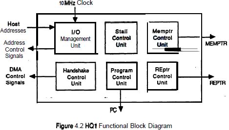 I/O Management Unit Responsible for providing address decoding and bus control for hardware accesses by the Host Interface Subsystem and Geometry Engine. Handshake Control Unit Used to provide necessary hardware handshake signals between Host Interface Subsystem, Raster Engine (RE) in the Raster Subsystem, microcode code and data RAM and XMAP2 or XPCl chips in Display Subsystem. It stalls GE5 when appropriate and passes other handshakes through for accesses such as host to XMAP or host to RE. The handshake control unit allows two types of transfers between the Host Interface Subsystem and the other MGR Subsystems. These two types of transfers are single word transfers and DMA transfers. Stall Control Unit Responsible for stalling the GE5 when a condition arises that requires it to be stalled. The full stall keeps the I/O Management unit in its current state and also keeps the PC, MEMPTR and REPTR from changing. The clock to the Weitek 3132 is fully suppressed and the entire GE5 is literally stalled. PC Control Unit Acts as a microcode sequencer for the GE5. The control unit controls microcode instruction execution sequencing through up to 32K words of microcode. The PC control unit allows branching and conditional jumps. It uses a 15 bit wide PC to access microcode code RAM. Microcode instructions are read from the address pointed to by the PC and are executed by the HQ1 and the Weitek 3132 chip. MEMPTR Control Unit Used as a data pointer for accessing words in microcode data RAM. MEMPTR is 14 bits wide allowing a maximum microcode data RAM size of 16K words. The MGR has only 8K words of microcode data RAM and each microcode data RAM word is 32 bits wide. The MEMPTR is loaded from microcode instructions to perform microcode data RAM accesses by the microcode. REPTR Control Unit Used as an address pointer to RE registers. It is used by GE5 microcode to load RE registers. REPTR is not accessible by host which means that host cannot directly access RE registers. A microcode token GE_LOADRE allows the host to load RE registers with an assist from microcode. The host generally does not access RE register directly and exceptions will be discussed later. GE Data Bus Buffer This is a 32 bit buffer which allows data to be passed between the GE5 bus and the host interface. Single word transfers use this data path to transfer data between the host and the microcode code RAM, the microcode data RAM and the HQ1 PC register. DMA transfers between the host and the microcode data RAM or between the host and the Raster Engine also use this data path. Utility Bus Buffer This is an eight bit transceiver which allows data to pass between the host bus and the utility bus. Only the low byte of the local bus are passed on to the utility bus. The address decoding and control signal generation are handled by the HQ1. IrisVision Board Functional Diagrams   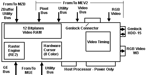
IRISVISION VIDEO TIMING PARAMETERS Original HERE
ADF Sections AdapterId 8EE6h "SGI Micro-Channel IRISVISION Adapter" Interrupt Level Memory Mapped I/O Address
Range Arbitration Level |
||||||||||||||||||||||||||||||||||||||||||||||||||||||||||||||||||||||||||||||||||||||||||||||||||||||||||||||