|
Trademark Info "sabine" or "High Performance 3D Color Graphics Processor".devices.mca.8ee6 Roger Brown's Site via Internet Archive The
Very
Unofficial IrisVison Home Page By
Roger Brown IV1WinSrc.zip
IrisVision Win 3.1 driver source - Thanks to
Resman (Glory be unto him!) IrisVision drivers and related
software: Note to PS/2 MicroChannel
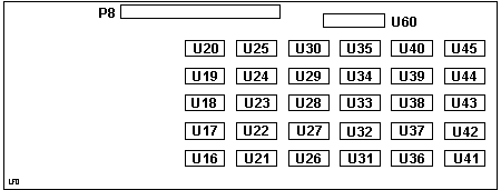
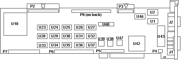
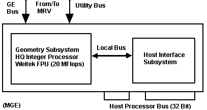
Users: IRISVISION Owner's Guide IRISVIEW User Guide ADI Driver User's Guide From Roger Brown: IrisVision Technical Reference. About 700 pages. irisvision_technical_reference_toc.pdf 393,985 irisvision_technical_reference_1.pdf 30,153 irisvision_technical_reference_2.pdf 130,719 irisvision_technical_reference_3.pdf 894,054 irisvision_technical_reference_4.pdf 2,819,748 irisvision_technical_reference_5.pdf 7,749,509 irisvision_technical_reference_6.pdf 12,319,323 irisvision_technical_reference_7.pdf 7,216,138 IrisVision Cards IRISVision General Components 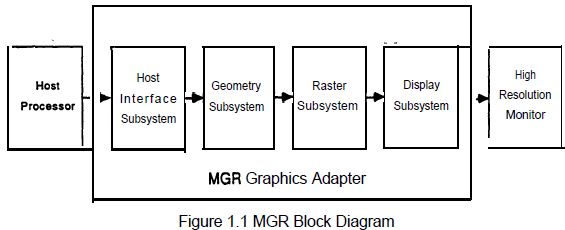 MGE2 Geometry Engine (Card has both GE and HI) The Host Interface subsystem interfaces to the host processor via the Micro Channel Architecture (MCA) bus. It provides all of the necessary data and control signals required by the MCA bus. It also interfaces to the other three subsystems over a local bus which is compatible with the SGI private bus. The Host Interface Subsystem provides the programmable Option Select (POS) registers which are used to configure the MCA bus interface aspects of the adapter. MGE2 Geometry Engine (Card has both GE and HI) The Geometry subsystem contains the Geometry Engine which is used to perform the geometric transformations and lighting calculations on the graphics data. It also performs the clipping and high level rendering calculations before sending the data to the Raster subsystem. The Geometry Engine performs high speed floating point calculations under the control of the onboard microcode. The host system issues commands to the Geometry Engine by sending command tokens and data parameters down a FIFO. The Geometry Engine reads the FIFO and performs the desired functions. The Geometry Subsystem also contains hardware which controls the addressing of the hardware components in the Raster and Display Subsystems. MRV2 Raster Video (both Raster and Display
Subsystems) The Raster Subsystem provides the necessary data and control signals to manage the frame buffer bitplanes as well as the Window ID bitplanes and the Auxiliary bitplanes. The Window ID bitplanes are used to control the display format for up to sixteen different on screen windows. The Auxiliary bitplanes are used for drawing pop-up menus, overlays and underlays. The Raster Subsystem also contains two hardware cursor chips. MRV2 Raster Video (both Raster and Display
Subsystems) The Display Subsystem performs the necessary
operations to access the frame buffer as a single buffer
or as a double buffer. The Digital-to-Analog Converters
(DACs) are used to convert the digital RGB data into
analog RGB data which output to the monitor. The Display
Subsystem also provides the necessary timing signals to
allow four different types of monitors to be connected
to the adapter. MEV2 24 Bit Video Option FRU: 71F1114 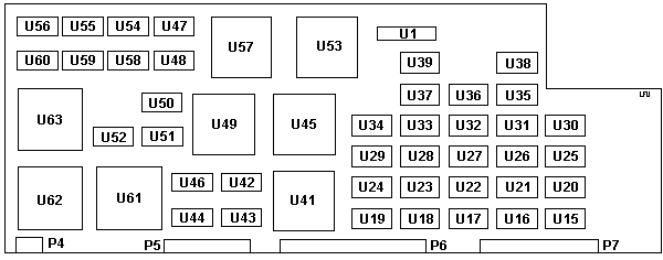
Bt457KPJ125 125 MHz Monolithic CMOS 256 Color Palette RAMDAC Datasheet This card supplies additional bitplanes of memory to bring the system to 24 bits per pixel of normal framebuffer in addition to 2 additional overlay/popup bitplanes and 2 additional window ID planes, for a total of 32-bits per pixel. A fully configured frame buffer has a total of 1280x1024*(32/8) or 5MB of video RAM (VRAM) implemented in 256Kx8 ICs. You'll notice that the VRAM is laid out in a 5xN array of chips. Each chip supplies 256 horizontal pixels (1280/5 = 256). However, to achieve greater performance, the raster engine chip is designed to write up to 5 pixels at a time, so the five VRAM chips are interleaved; the first supplies pixels 1, 6, 11, etc. the second 2, 7, 12, etc. and so on. The MEV2 card is a daughter board which attaches to the MRV2 card. It has a VPD PROM and provides an additional 20 bitplanes of VRAM which are part of the Raster subsystem. It also contains the five XMAPP2 chips, the 8K color map chip and the three DAC chips which are part of the Display subsystem and are described in the chapter on the Display subsystem. The card has the Utility bus, Video bus, Pixel bus and RGB connections described above for the MRV2 card. ISA vs MCA MEV2 MEV2 ISA 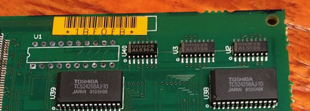 MEV2 MCA 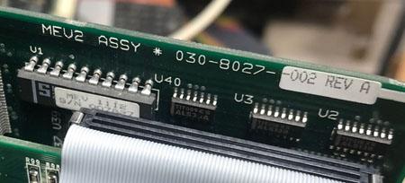 Of course, the internal traces may be different, but the PCB layouts sure look the same, except the ISA version lacks U1 [not needed for ISA]. MZB1
24 Bit Video Buffer FRU: 42F6889
This is the optional 24-bit hardware z-buffer card. The function of the z-buffer is to perform hidden surface removal via a depth test mechanism. In the traditional application, each pixel's "Z" coordinate value is tested against the value already present in that location in the z-buffer. If it is smaller (i.e. closer to the eye) the pixel is updated with the current value and the z-buffer is updated. By controlling the z-buffer operation, a number of other useful operations can performed. For non-3D applications, the z-buffer can be used as an off-screen memory buffer for saving the contents of the normal framebuffer. As no host to adapter memory transfer takes place, this operation is very fast. The z-buffer is implemented in dynamic RAM (DRAM) and consists of 3.75 MB of DRAM. MRV2 Raster Video FRU: 71F1151
Bt431KJP Monolithic CMOS 64x64
Pixel Cursor Generator Datasheet
30MHz osc - 15MHz for PAL and
SECAM MC10H115P Quad Line Receiver This is the
MicroChannel Raster Video Engine. It is based upon the
RE 2.1 raster engine chip from SGI. The raster engine
provides all the per-fragment and -pixel operations.
It also contains the raster scanning hardware and
video signal generation circuitry. It only obtains
power and ground from the bus, no other bus signals
are used. In addition to the two ribbon cables from
the Geometry Engine, a third connection services the
Genlock features of the Raster Engine. 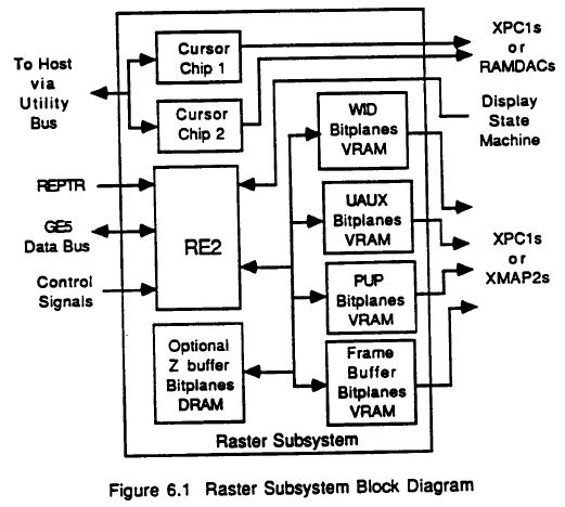 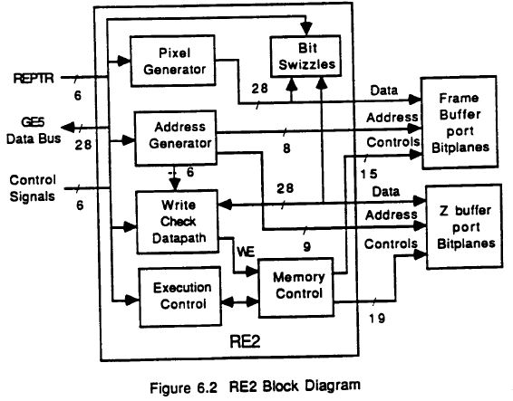 
The Display State Machine (DSM) is
built out of a XILINX 2018 programmable logic array, an
8K by 8-bit RAM, a Bt438 clock generator chip and other
miscellaneous clock control circuitry. The 8K PROM
contains the Xilinx logic configuration data and the
four different monitor timing tables. On system reset
the logic configuration is loaded into the Xilinx chip
and the monitor timing tables are copied to the 2K RAM
for faster access. The operation of the DSM is
controlled by various bits in the display registers.
On the card edge
connector, are the VGA passthrough connector and the
HiRes video output connector. The Raster Video card
contains the basic 8-bitplanes of framebuffer memory
as well as 2 bitplanes of overlay framebuffer and 2
bits of window ID bitplanes, for a total of 12 bpp. 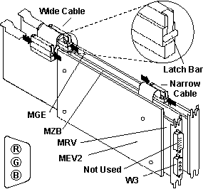 Connector cable (wide) 53F3271 80 pin .025 pitch HPDB Connector cable (narrow) 53F3272 40 pin .025 pitch HPDB Removing Connector Cable
Plugging Connector Cables Back
On The following block diagram is derived from the
IrisVision Block Diagram on The
Very
Unofficial IrisVison Home Page IrisVision Board Functional Diagrams 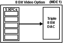 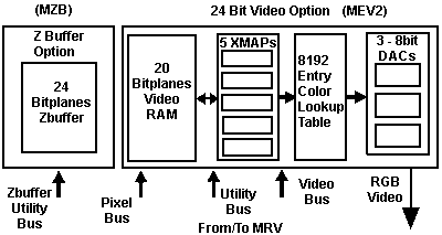 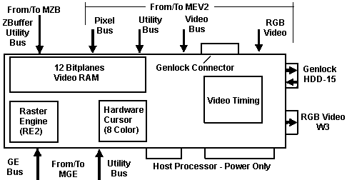
Product Description: Stolen from Roger Brown's The Very Unofficial IrisVison Home Page Hardware: Notable differences from the Personal Iris graphics
are: The card has a rich set of video and rendering modes consistent with the Personal Iris. Origins of the IrisVision
In the process of testing the product, it was discovered that an IBM PS/2 model 70 personal computer running OS/2 could be used to run diagnostics and test programs on the card much easier than using the RS-6000. So a minimal device driver was written for the card and soon IBM was shipping product. (Ed. Roger Brown can't find the "minimal OS/2 drivers" and he works for SGI.) At some point, the light went off in
someone's head; "Why don't we sell this board set for
use in PCs?". IrisVision was born. Initially, the MCA
card was re-designed to offer some features critical for
the PC market, including standard 15-pin VGA-style video
output and a 15-pin VGA passthrough input connector. The
IBM genlock connector was moved to the top of the card,
and stereo display signals were also brought out to the
VGA passthrough connector. The card occupied 1 32-bit
MCA slot and an adjacent 16/32 bit slot. One or two
daughter boards provided framebuffer and z-buffer
memory. Work then began on the design of an Industry Standard Architecture (ISA or AT-bus) version of the card. It would occupy 2 16-bit ISA slots and use the identical daughter cards as the MCA (and IBM) versions of the board set. Software: IRISVISION VIDEO TIMING PARAMETERS Original HERE
ADF Sections AdapterId 8EE6h "SGI Micro-Channel IRISVISION Adapter" Interrupt Level Memory Mapped I/O Address
Range Arbitration Level Trademarks Silicon Graphics, SGI, OpenGL, Personal Iris, and IrisVision are registered trademarks of Silicon Graphics, Inc. I usually don't mess with Trademarks, but that of SGI is very classy Trademark Info just was too damn good. Class act, SGI! I wish M$ and their bloodsucking shark team was only a tenth as smooth as you! Sorry, SGI, Netscape makes them durned TM's and Registered marks look like ASCII. SGI does not endorse any of the information on this page. They retain all rights to their trademarks. Further, this information is furnished on an "As Is" basis. If you fry your monitor or card, that's your problem. |
||||||||||||||||||||||||||||||||||||||||||||||||||||||||||||||||||||||||||||||||||||||||||||||||||||||||||||||||||